MCU land, part 8: DMA bit-vending machines
How to dispense data with the push of a button, and why it's useful for interfacing your microcontroller to the outside world.
In one of the earlier installments of the series, I discussed the Direct Memory Access (DMA) subsystem on a family of high-performance, 32-bit Cortex-M7 microcontrollers made by Microchip.
The extended DMA controller (XDMAC) available on these devices performs on-demand memory transfers without the involvement of the CPU core. More interestingly, the XDMAC can be also instructed to move data between memory and I/O ports, synchronizing this operation to hardware signals — for example, to match the transmit speed of the Serial Peripheral Interface (SPI) bus.
Alas, for all their utility, DMA controllers tend to be inflexible beasts: for example, the XDMAC on SAM E70 / S70 / V70 MCUs supports a total of 51 synchronization sources, but not a single one is suited for ad-hoc experimentation. In particular, there is no way to build a “bit-vending machine”: a contraption that, with every press of a button, sequentially dispenses data from memory in a format of our choice without having to involve the CPU.
The idea might sound silly, but this functionality is an essential building block for adding DMA support to any communication protocols that aren’t already baked onto the chip. As an example, consider that many higher-resolution TFT displays don’t have internal framebuffers and require a constant stream of RGB values to be sent through a parallel data bus at a multi-megahertz “pixel clock” frequency. Driving such a display via an interrupt routine or a synchronous event loop would be burdensome; but a DMA channel synchronized to a pixel clock could conceivably give us full-color display practically for free, even if the MCU has no hardware support for a display module.
In this article, let’s have a look at how we can work around these limitations and get what we want.
Exploring the PIODCCLK route
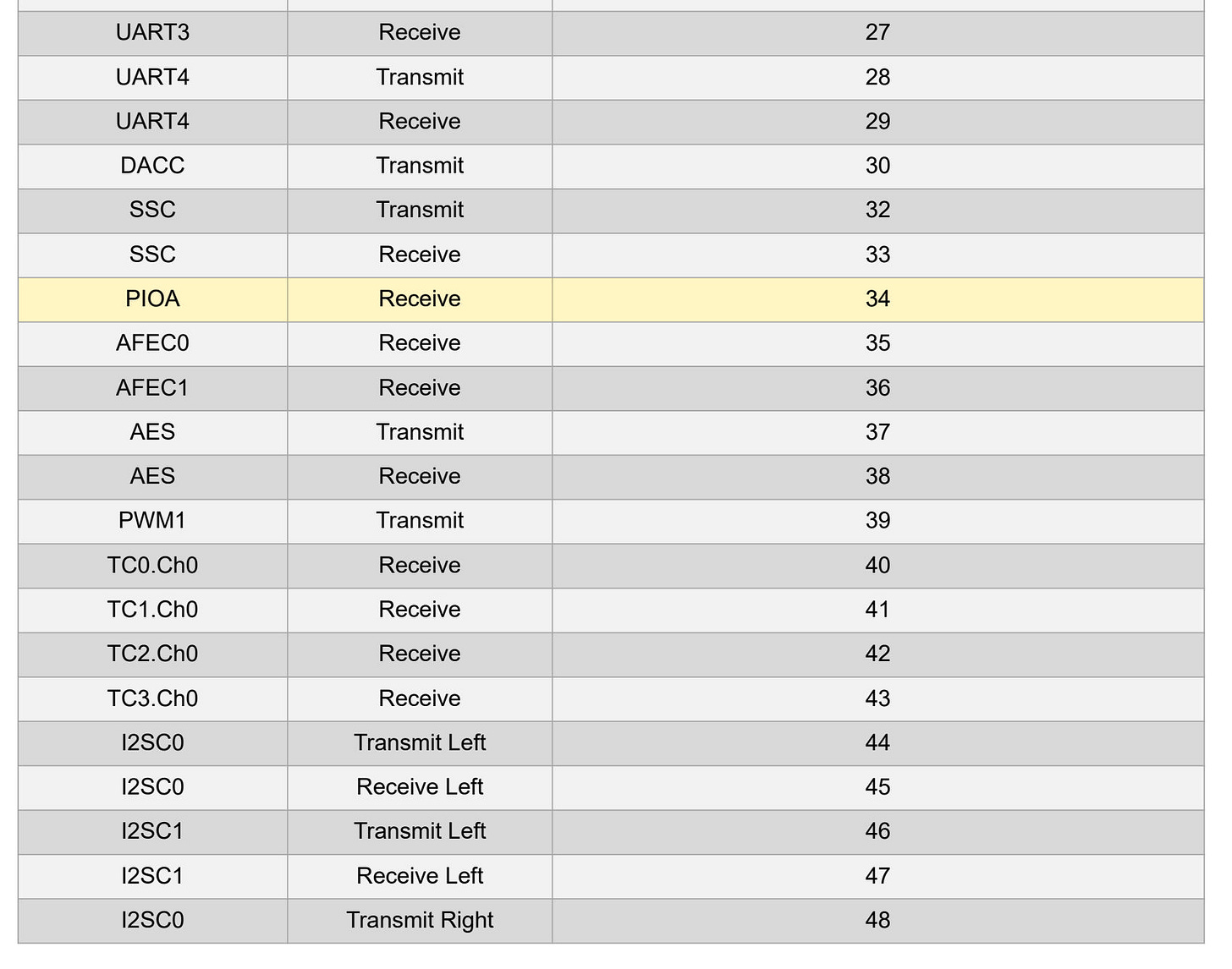
While perusing the SAMS70J21B datasheet, it caught my eye that you can select PIOA — parallel I/O controller, port A — as one of the data transfer sync sources for the XDMAC:
Hmm… how does a port controller generate a DMA synchronization signal? Well, as it turns out, this feature is meant to support parallel data capture for CMOS image sensors. In this setup, the MCU is provided with an external clock on the PIODCCLK line (pin 17 in the LQFP-64 package). If the PIOA is configured for parallel capture, the controller recognizes this signal, loads the input data from nearby pins into the PIO_PCRHR register, and then tells the DMA controller to copy the register into main memory.
There doesn’t appear to be a complementary mode for sending data, but perhaps we can instruct the XDMAC to move data between different endpoints while still using PIODCCLK for sync (#34)? Let’s try that, starting with a generic function to request a peripheral-synchronized transfer (this is a slight revision of the code from an earlier article):
void turn_on_dma() {
  PMC->PMC_PCER1 = 1 << 26;
}

void dma_sync_send(uint8_t dma_ch, const void* src, volatile void* pio,
                   uint32_t len, u8 per_id) {
  uint32_t sif = 0;

  XDMAC->XdmacChid[dma_ch].XDMAC_CSA  = (u32)src;
  XDMAC->XdmacChid[dma_ch].XDMAC_CDA  = (u32)pio;
  XDMAC->XdmacChid[dma_ch].XDMAC_CUBC = len;

  /* Check if the source is in flash; if yes, we need to use DMA iface #1 */
  if ((u32)src < 0x20400000) sif = (1 << 13);

  XDMAC->XdmacChid[dma_ch].XDMAC_CC =
    (1)            /* TYPE: peripheral-synchronized */ |
    (1 << 4)       /* DSYNC: sync before write */ |
    (0 << 11)      /* DWIDTH: bytes */ |
    sif            /* SIF: source on DMA interface #0 or #1 (see above) */ |
    (1 << 14)      /* DIF: destination on DMA interface #1 */ |
    (1 << 16)      /* SAM: source address increment */ |
    (0 << 18)      /* DAM: destination address fixed */ |
    (per_id << 24) /* PERID: sync peripheral ID */;

  XDMAC->XDMAC_GE = (1 << dma_ch); /* Go! */

}
Next, let’s enable the PIOA controller, turn on the parallel capture mode (PCEN), connect a LED to port PD3 (pin 55 in the LQFP-64 package), and see if we can get the DMA controller to produce a sequence of blinks:
#define PD_LED (1 << 3)

static const uint8_t led_blinks[10] =
  { 0, PD_LED, 0, PD_LED, PD_LED, 0, PD_LED, PD_LED, PD_LED, 0 };

...

PMC->PMC_PCER0  = 1 << 10;  /* Enable PIOA controller          */
PIOA->PIO_PCMR  = (1 << 9); /* ALWYS=1: ignore enable lines    */
PIOA->PIO_PCMR |= 1;        /* PCEN=1: enable parallel capture */

PIOD->PIO_OER  = (1 << 3);  /* Enable output on PD3     */
PIOD->PIO_PUDR = (1 << 3);  /* Disable PD3 pull-up      */
PIOD->PIO_OWER = (1 << 3);  /* Enable synchronous write */

turn_on_dma();
dma_sync_send(0, led_blinks, &PIOD->PIO_ODSR, sizeof(led_blinks), 34);
Unfortunately, this doesn’t work! Although the spec doesn’t really spell it out, I eventually figured out there is a handshake protocol between the XDMAC and the PIOA: once the first DMA sync request is generated, no further requests will go through until the XDMAC actually touches the PIO_PCRHR register.
Although this problem can’t be easily solved within the DMA request we’re trying to make, the MCU has 24 DMA channels — and we can easily program a second, dummy DMA request that triggers on the same sync signal, then performs a read from PIO_PCRHR to get things unstuck. A generic function to configure a dummy transfer might look like this:
void dma_dummy_recv(uint8_t dma_ch, volatile const void* pio,
                    volatile void* dst, uint32_t len, uint8_t sync_src) {

  XDMAC->XdmacChid[dma_ch].XDMAC_CSA  = (u32)pio;
  XDMAC->XdmacChid[dma_ch].XDMAC_CDA  = (u32)dst;
  XDMAC->XdmacChid[dma_ch].XDMAC_CUBC = len;

  XDMAC->XdmacChid[dma_ch].XDMAC_CC =
    (1)       /* TYPE: peripheral-synchronized */ |
    (1 << 2)  /* MBSIZE: 4 bytes */ |
    (0 << 4)  /* DSYNC: sync before read */ |
    (0 << 11) /* DWIDTH: bytes */ |
    (1 << 13) /* SIF: source on DMA interface #1 */ |
    (1 << 14) /* DIF: destination on DMA interface #1 */ |
    (0 << 16) /* SAM: source address fixed */ |
    (0 << 18) /* DAM: destination address fixed */ |
    (sync_src << 24) /* PERID: sync peripheral ID */;

  XDMAC->XDMAC_GE = (1 << dma_ch); /* Go! */

}
With this code in place, we can add the following lines at the end of our program to make the bit-vending machine work:
...

static volatile uint8_t dummy;
dma_dummy_recv(1, &PIOA->PIO_PCRHR, &dummy, sizeof(led_blinks), 34);
In this design, there is an end-to-end latency of about 90 nanoseconds between the falling edge of the externally-provided PIODCCLK signal and a bit flip on the output pin:
It follows that the maximum stable transfer speed is about 10 MHz.
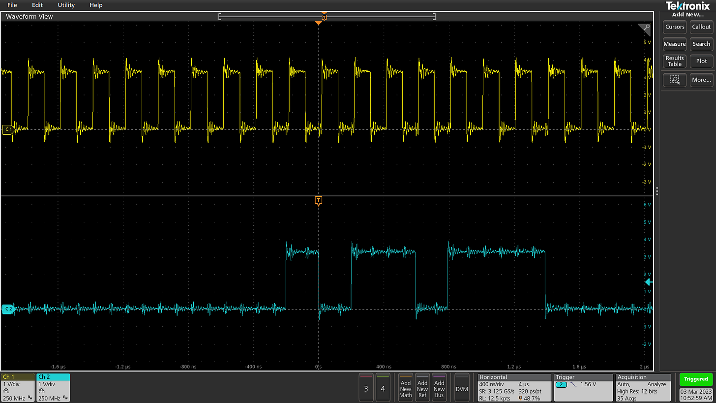
Here’s a capture of a 6 MHz PIODCCLK signal (yellow) and the DMA-mediated output sequence on PD3 (blue). The signal shows excellent timing stability and somewhere around 50% phase lag:
Up to 32 bits can be pushed out with a single DMA operation, so transfer rates of around 320 Mbit/sec from SRAM should be attainable. Not too shabby for an approach that has the CPU core just sitting there fiddling its thumbs!
Switching to a built-in clock
Although the PIODCCLK solution is cute, it depends on an external clock — so instead of quitting while I’m ahead, I set out to figure out if it’d be possible to switch to an internally-generated time reference.
The SAM S70 chip has a built-in PWM module, capable of generating a variety of complex clock signals; the module also happens to have a hardware line to the XDMAC. But once again, the purpose of this line is different from what we need: the intended use case is automatically loading values from memory into the PWM duty cycle register. This is useful for tasks such as 1-bit analog-to-digital or digital-to-analog conversions, certain types of radio modulation, and so forth.
To see how far we can get with this, let’s set up a simple PWM waveform, output it on PA11 (pin 27), and configure the XDMAC to perform an unrelated transfer while keying it off the PWM sync line (#13):
#define PD_LED (1 << 3)

static const uint8_t led_blinks[10] =
  { 0, PD_LED, 0, PD_LED, PD_LED, 0, PD_LED, PD_LED, PD_LED, 0 };

...

PMC->PMC_PCER0 = (1 << 10); /* Enable PIOA controller */
PMC->PMC_PCER0 = (1 << 31); /* Enable PWM0 controller */

/* Disable PIOA control of PA11 (LQFP-64 pin 27) */
PIOA->PIO_PDR  = (1 << 11);

/* Enable PA11 alternate function B (PWM output). */
PIOA->PIO_ABCDSR[0] = (1 << 11);
PIOA->PIO_ABCDSR[1] = 0;

PIOD->PIO_OER  = (1 << 3);  /* Enable output on PD3     */
PIOD->PIO_PUDR = (1 << 3);  /* Disable PD3 pull-up      */
PIOD->PIO_OWER = (1 << 3);  /* Enable synchronous write */

/* PWM0 channel 0: system bus clock, 200 tick period, 50% duty cycle */
PWM0->PwmChNum[0].PWM_CDTY = 100;
PWM0->PwmChNum[0].PWM_CPRD = 200;

/* Automatic DMA updates of channel 0 (UPDM=2, PTRM=0, SYNC0=1) */
PWM0->PWM_SCM = (2 << 16) | (0 << 20) | 1;
PWM0->PWM_ENA = 1;

turn_on_dma();
dma_sync_send(0, led_blinks, &PIOD->PIO_ODSR, sizeof(led_blinks), 13);
It’s probably no surprise that this code fails to transmit the desired sequence on the output pin (PD3). Once again, the PWM controller is waiting for the XDMAC to take a specific action before sending any additional requests; in this case, it expects a new duty cycle value to be written to PWM_DMAR (from where it is eventually loaded into PWM_CDTY).
So, let’s clobber together another dummy DMA request, this time to perform a pointless 32-bit register write:
void dma_dummy_send32(uint8_t dma_ch, const void* src, volatile void* pio,
                      uint32_t cnt, uint8_t sync_src) {

  XDMAC->XdmacChid[dma_ch].XDMAC_CSA  = (u32)src;
  XDMAC->XdmacChid[dma_ch].XDMAC_CDA  = (u32)pio;
  XDMAC->XdmacChid[dma_ch].XDMAC_CUBC = cnt;

  XDMAC->XdmacChid[dma_ch].XDMAC_CC =
    (1)       /* TYPE: peripheral-synchronized */ |
    (1 << 2)  /* MBSIZE: 4 bytes */ |
    (1 << 4)  /* DSYNC: sync before write */ |
    (2 << 11) /* DWIDTH: 4 bytes */ |
    (1 << 13) /* SIF: source on DMA interface #1 */ |
    (1 << 14) /* DIF: destination on DMA interface #1 */ |
    (0 << 16) /* SAM: source address fixed */ |
    (0 << 18) /* DAM: destination address fixed */ |
    (sync_src << 24) /* PERID: sync peripheral ID */;

  XDMAC->XDMAC_GE = (1 << dma_ch); /* Go! */

}
Now, we just need to add a couple of lines at the very end of our code:
...

static const uint32_t dummy_duty = 100;
dma_dummy_send32(1, &dummy_duty, &PWM0->PWM_DMAR, sizeof(led_blinks), 13);
It works! Compared to the PIODCCLK experiment, with PWM-based sync, the propagation latency appears to be a bit higher, and the maximum attainable clock speed appears to be around 7 MHz. Here’s a plot of the PWM signal on PA11 (yellow) next to the DMA transmission on PD3 (blue):
The SAM S70 PWM controller allows a considerable number of additional synchronized clock signals to be derived from a common base, with varying duty cycles and other characteristics. For the TFT pixel clock use case in particular, generating the required HSYNC or DEN signals should be a breeze.
Precisely-timed data transfers are the lifeblood of digital circuits, and recruiting a DMA controller to help with such tasks can greatly simplify your code. And although DMA subsystems are not designed to be particularly flexible… life, uh, finds a way.
👉 To check out earlier MCU- and electronics-related articles on this blog, please visit this page.


OMG Thank you SO much...I've been fighting with this for a week!!
Excellent article.