Some time ago, my eldest son decided to build a single-bit computer using discrete transistors. The idea of a one-bit device might sound wacky, but the moniker doesn’t refer to a machine that can only have two instructions or two memory cells. Instead, it stands for the “word” size of the arithmetic logic unit (ALU). Low bit widths result in simpler circuitry, but require any operands wider than the hardware limit to be processed in steps. One-bit ALUs are a bit extreme, but they have commercial precedent — notably including the MC14500B microcontroller made by Motorola in the late 1970s.
That said, today’s post is about something else: as dictated by the iron laws of sibling rivalry, his younger brother soon approached me and asked if I could help him build a computing device that’s even more obsolete. After some back-and-forth, we settled on a relay-based calculator. I was given further instructions: the PCBs must be old-school and off-yellow, and all relays must be see-through.
From the get go, I knew we wouldn’t be building a circuit that’s 100% relay-based. Doing so would make the project drag on for months — and especially with these transparent relays that retail for $6 a piece, it would cost too much. Still, I figured we can employ relays to do the actual math!
A quick refresher on ALUs
One of the most fundamental building blocks of any electronic computing device is the adder circuit. Despite its unassuming name, the circuit is also sufficient to also implement subtraction, multiplication, and division of integers. A modern ALU will typically contain a variety of other arithmetic circuits too, but the adder is still a major star.
The addition of binary digits is conceptually similar to working with decimal numbers, except dumbed down. You have two inputs with two possible values each; there is one output digit with the same property; and there’s a carry bit that can be either propagated to the next column or used to signal an overflow. The behavior can be summed up using the following truth table:
 In_A  | In_B  | Out   | Out_C
-------+-------+-------+-------
 0     | 0     | 0     | 0
 0     | 1     | 1     | 0
 1     | 0     | 1     | 0
 1     | 1     | 0     | 1
This is notionally an arithmetic operation, but a cursory glance at the two rightmost columns reveals that it can be implemented using simple Boolean logic:
Out   = In_A XOR In_B
Out_C = In_A AND In_B
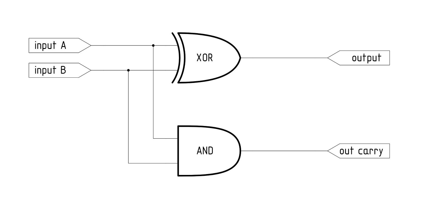
In an electronic circuit, if you have a way to construct basic logic gates, the obvious facsimile is:
That said, this circuit (a “half adder”) is incomplete in the sense that it doesn’t have a way to take carry from the preceding column into account; in other words, it can’t automatically add multi-digit integers.
To build a complete (“full”) adder, we need to take a somewhat more complicated approach with a third input line:
 In_A  | In_B  | In_C  | Out   | Out_C
-------+-------+-------+-------+-------
 0     | 0     | 0     | 0     | 0
 0     | 1     | 0     | 1     | 0
 1     | 0     | 0     | 1     | 0
 1     | 1     | 0     | 0     | 1
       |       |       |       |
 0     | 0     | 1     | 1     | 0
 0     | 1     | 1     | 0     | 1
 1     | 0     | 1     | 0     | 1
 1     | 1     | 1     | 1     | 1
The first half (In_C = 0) is the same as for a half adder. The second half differs: in the presence of input carry, the output is inverted, and the carry propagates in all cases except In_A = In_B = 0. The equivalent Boolean algebra is less elegant, but still easy to reverse-engineer:
Out   = (In_A XOR In_B) XOR In_C
Out_C = (In_A AND In_B) OR (In_C AND (In_A OR In_B))
The electronic implementation can be realized by following this formula verbatim. Alternately, it can be imagined as two half adders chained together, plus an OR operation applied to their carry outputs:
Full adders can be stacked to add any number of binary digits at once. A single adder can be also used serially as a part of a 1-bit ALU — similar to my eldest son’s design mentioned earlier on.
Relay-based logic
Relays have two properties that make them well-suited for building digital logic: they are inherently binary in their operation, and they can “amplify” input signals so that you can chain the devices indefinitely. (To be fair, relays also have a number of disadvantages: they are slow, costly, loud, and their contacts are prone to wear.)
There are many ways to implement relay-based logic, in part because of the variety of relays on the market and all the different ways of encoding zeroes and ones. For example, Konrad Zuse’s Z3 computer relied on exotic four-pole double-throw (4PDT) devices and “cheated” by also propagating a secondary, inverted carry signal — but the design pulled off a full adder with just two relays!
For my project, using the lowest possible number of relays wasn’t a particularly appealing goal. Instead, I wanted to stick to commodity parts and keep the layout clean. I also had the aforementioned requirement for relays with see-through housings.
After some research, I settled on a series of compact G6C relays from Omron. The devices are available with a single SPST-NO switch, or with a complementary pair of SPST-NO and SPST-NC terminals. Here’s the SPST-NO design I used for the OR gate:
The operation of this circuit should be obvious: the output is connected to the positive supply rail if either of the relays is on. Otherwise, the output floats.
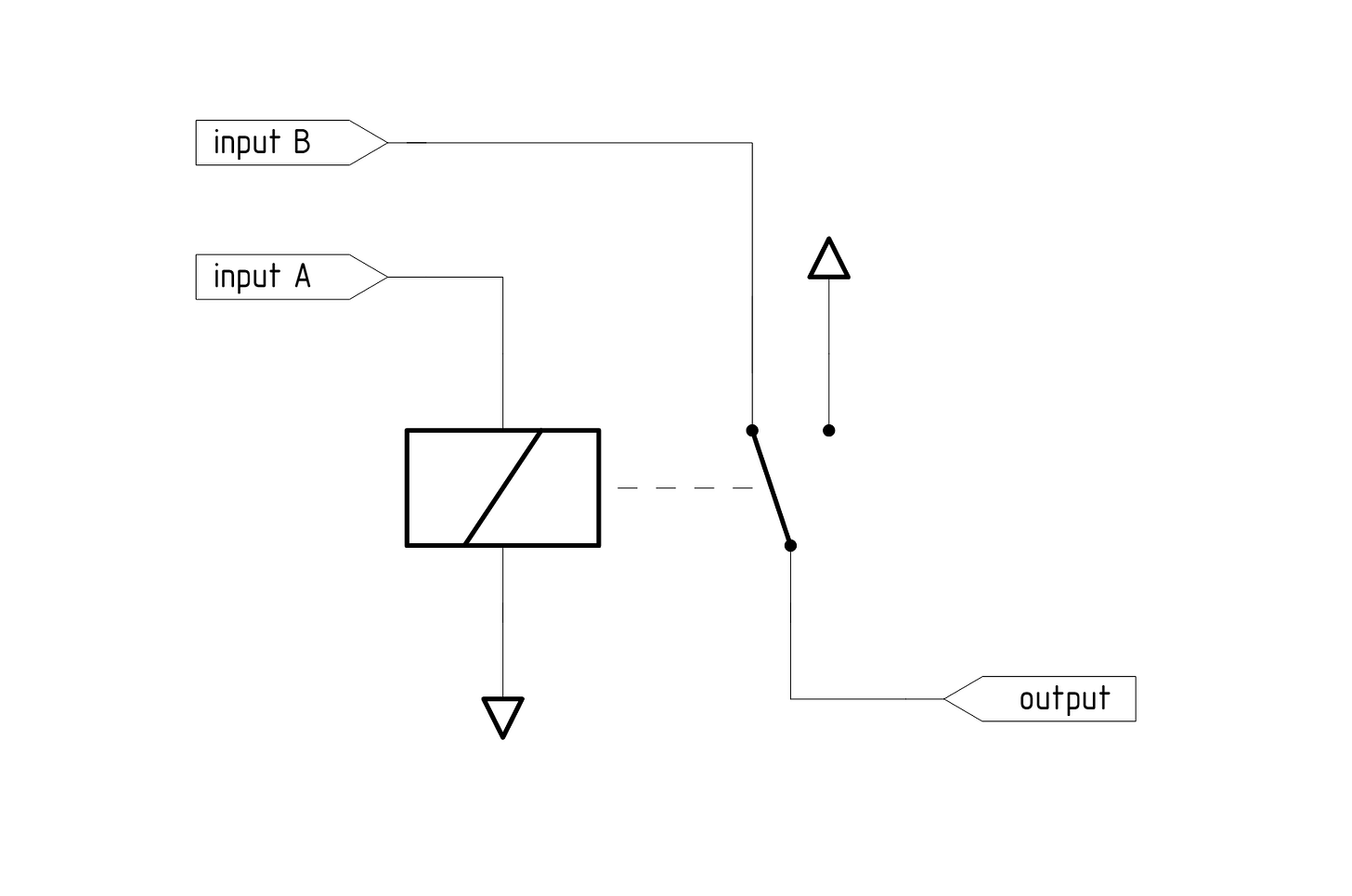
One could also implement an OR gate with a single SPDT relay, although the pass-through architecture for one of the inputs means that “fanout” (downstream loading of the output) must be kept in check:
An AND gate can be constructed similarly, with one or two SPST-NO relays:
The construction of an XOR gate is a bit more involved, generally benefiting from double-throw relays. Here’s the solution I implemented with Omron’s complementary SPST-NO + SPST-NC topology:
The SPST-NO terminals perform an OR operation, connecting the output to a common rail (bottom) when any of the relays is on. The SPST-NC side performs NAND, disconnecting that rail from the positive supply when both relays are energized.
A more compact version of essentially the same architecture can be drawn with SPDT relays, as shown below:
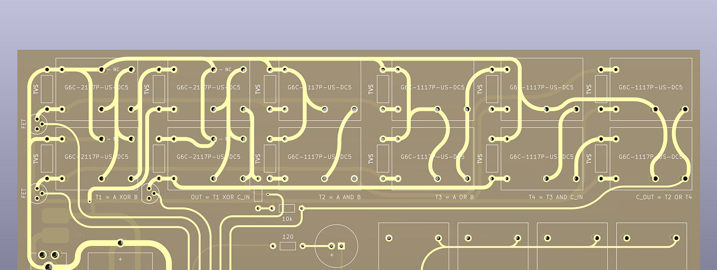
In the end, I used twelve relays for the most straightforward implementation of the six Boolean operations needed to implement a full adder:
Out   = (In_A XOR In_B) XOR In_C
Out_C = (In_A AND In_B) OR (In_C AND (In_A OR In_B))
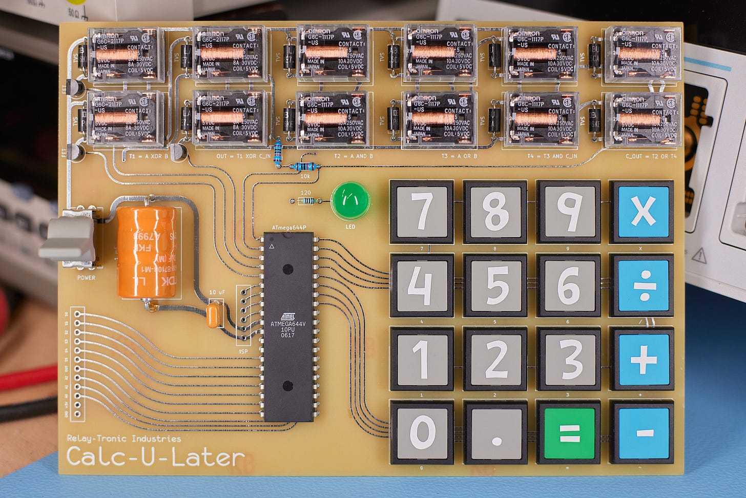
Here’s the close-up of the adder section on the PCB. Note the “retro” curved traces and the deliberate absence of a solder mask:
Getting this layout done in KiCad was an absolutely miserable experience. I had some extended back-and-forth with the PCB manufacturer too.
But it’s not just relays, right?
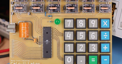
Nope, at least not for now! The entire “main” board is shown below, complete with homebrew keypad stickers, an old-school switch, a rare axial electrolytic cap — and yes, an 8-bit microcontroller:
The microcontroller is there to take care of a variety of auxiliary tasks that would require hundreds of additional relays. This includes keypad scanning, digit decoding, operation sequencing, error handling, and memory. That said, the adder has a clearly-delineated role and is there to perform actual math.
Here’s the sequence of MCU operations for addition:
Set operand bit pointer to 0 (LSB),
Initialize the adder “carry in” line to zero,
Push operand bits onto the adder input lines,
Wait around 20 ms for the relays to settle,
Read back and store the adder output bit,
Propagate “carry out” to “carry in”,
Advance the operand bit pointer to the right,
Loop back to #3 until out of bits to add.
In other words, there is no cheating, although the MCU could in principle do the ALU work on its own.
Of course, it’s not just addition; other arithmetic operations can be done with the same circuitry. For example, multiplication can be unwound into a series of progressive additions of bit-shifted values, somewhat akin to a dumbed-down version of how we do “long multiplication” by hand:
110 × 1011 = ?
 ↓     ↓
110 ×  1   →      110
110 ×  1   →     110
110 ×  0   →    000
110 ×  1   →   110
              -------
       sum =  1000010
This bit shifting can be done with an adder if one is so inclined; each left shift is equivalent to adding the operand to itself (i.e., multiplying it by 2).
Subtraction is similarly easy: it can be implemented the addition of two’s complement (which in turn can be computed by abusing the adder to operate as a NOT gate.) And with subtraction done, division is also within reach.
What about the display?
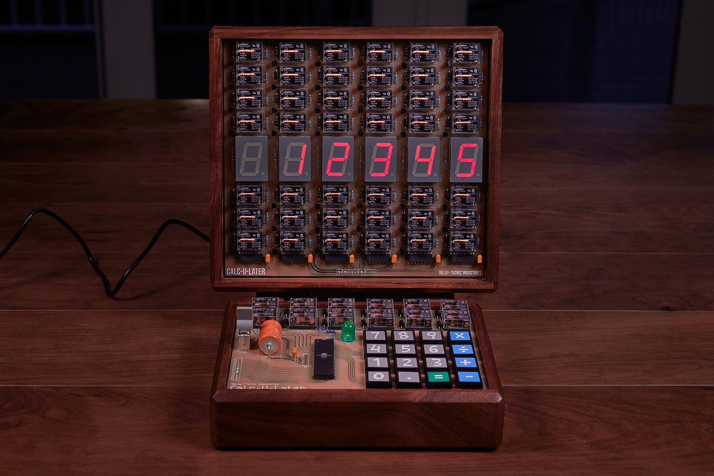
That’s where I went a bit nuts and constructed a Rube Goldberg-esque device just for the sake of it. The PCB contains a couple of 7-segment displays, but they are driven entirely by relays:
To keep the number of data lines in check, display state is stored in 8-bit latches (six 74HC259 chips at the bottom), so the relays are largely superfluous — but the idea was to make the entering digits as satisfying as watching the ALU at work.
Here’s an early video of a functional test of the display module:
The following audio-visually mesmerizing video shows the calculator handling the multiplication of 111 by 222:
Of course, for a project like this, we needed a suitable enclosure. We spent a couple of hours in the workshop to build this:
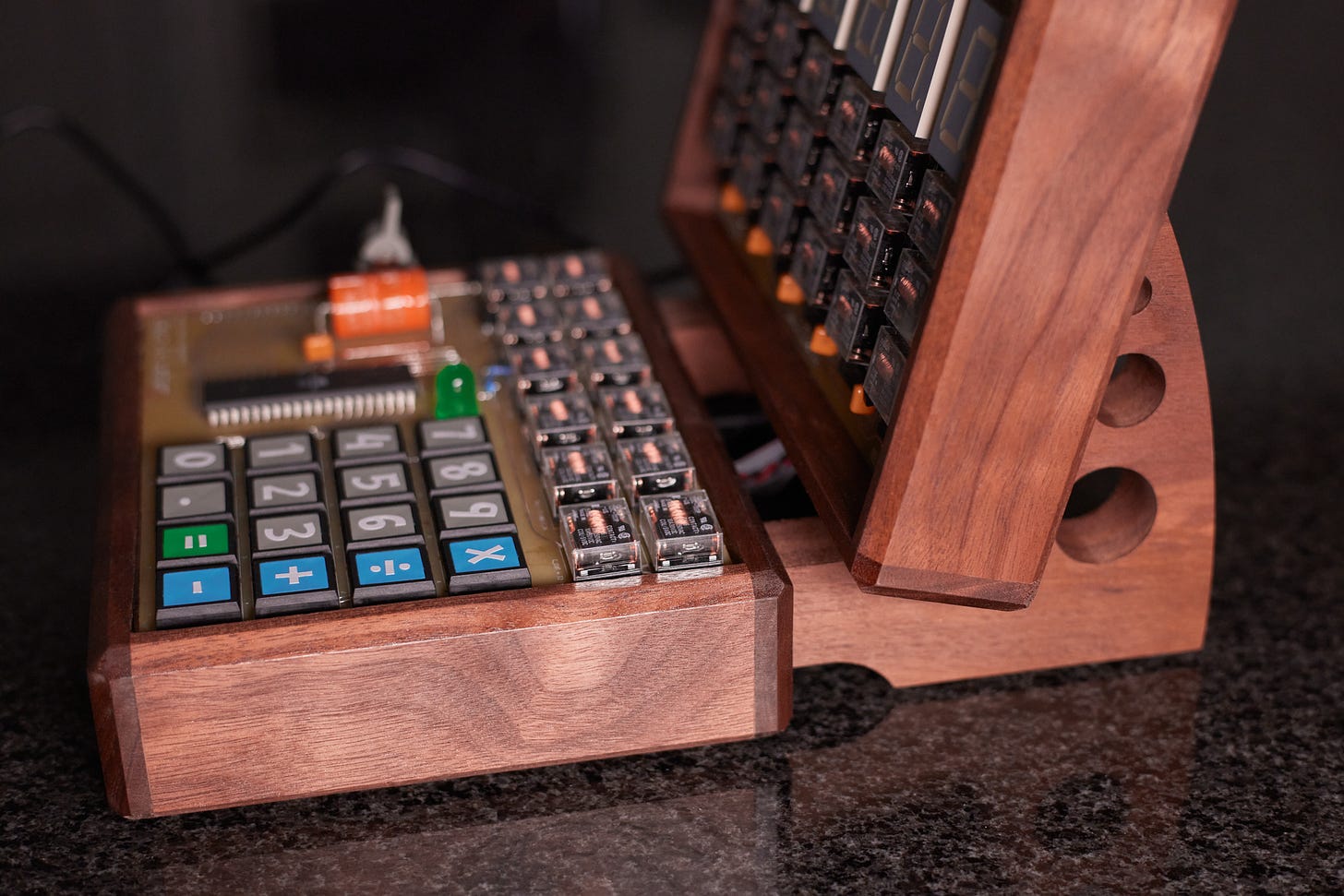
The front view doesn’t quite do this design justice; here’s a photo from the side:
Finally, here’s a video of the assembled calculator handling fractions, negative numbers, and division:
How many relays would you really need?
It depends. If we settle for primitive inputs and outputs — say, columns of fixed-position switches and indicators — then addition and subtraction can be done in a single step with an adder circuit of a sufficient width. The total number of relays would be a low multiple of the number of input bits.
The picture gets more complicated if we want to implement multiplication and division. These operations are most practically implemented as a series of steps. You’d need a clock, a “microcode sequencer”, and an array of multiplexers that flexibly connect registers to perform loads, stores, and ALU operations.
Even more complexity arises if we desire to support modern-style input, with digits typed in left-to-right. Because the operands need to be right-aligned for display and calculation, and the number of digits to be entered isn’t known beforehand, more circuitry would be needed to implement the necessary shifts.
In the end, precise estimates are hard, but extrapolating from early transistor calculators such as Friden EC-130, I’d wager that around 500 relays would be needed for the task.
At $6 a piece, the relays I’m using in this project wouldn’t be a wise choice; that said, subminiature signal relays, such as Kemet EA2-5NU, would result in a final price tag of under $1,000 — and in a reasonable desk footprint, too.
Power shouldn’t be a major issue — we’re talking tens of watts — but performance is a limiting factor. For subminiature relays, 50-100 Hz is probably the upper limit. For larger relays, 20 Hz is a lot.
Now that I have this “introductory” project wrapped up, I might be tempted to give a 100% relay-based calculator a try…
👉 You can download the source code for Calc-U-Later here. For a categorized list of my other articles on electronics, click here.
I write well-researched, original articles about geek culture, electronic circuit design, algorithms, and more. This day and age, it’s increasingly difficult to reach willing readers via social media and search. If you like the content, please subscribe!








Just for fun: a reader on Mastodon pointed me to https://github.com/olofk/serv, which is an attempt to implement a RISC-V CPU using the absolute minimum number of... well, things. I think their goal is to optimize FPGA implementations with LUTs and flip-flops, but they also have a CMOS estimate of 2,100 gates.
This is within the ballpark of what's still realistically possible with relay logic, so one could build a dreadfully slow RISC-V relay computer.
Any chance you could share the PCB?