
Cursed circuits #2: switched capacitor lowpass
Still using resistors? Get on with the times.
In the previous post on this Substack, we looked at charge pump circuits and the mildly cursed example of a capacitor-based voltage halver. I find these topologies interesting because they are very simple, yet they subvert the usual way of thinking about what a capacitors can or cannot do.
In today’s episode, let’s continue down that path and consider an even more perplexing example: a switched capacitor lowpass filter. The usual way to design an analog lowpass filter is to combine a resistor with a capacitor, as shown below:
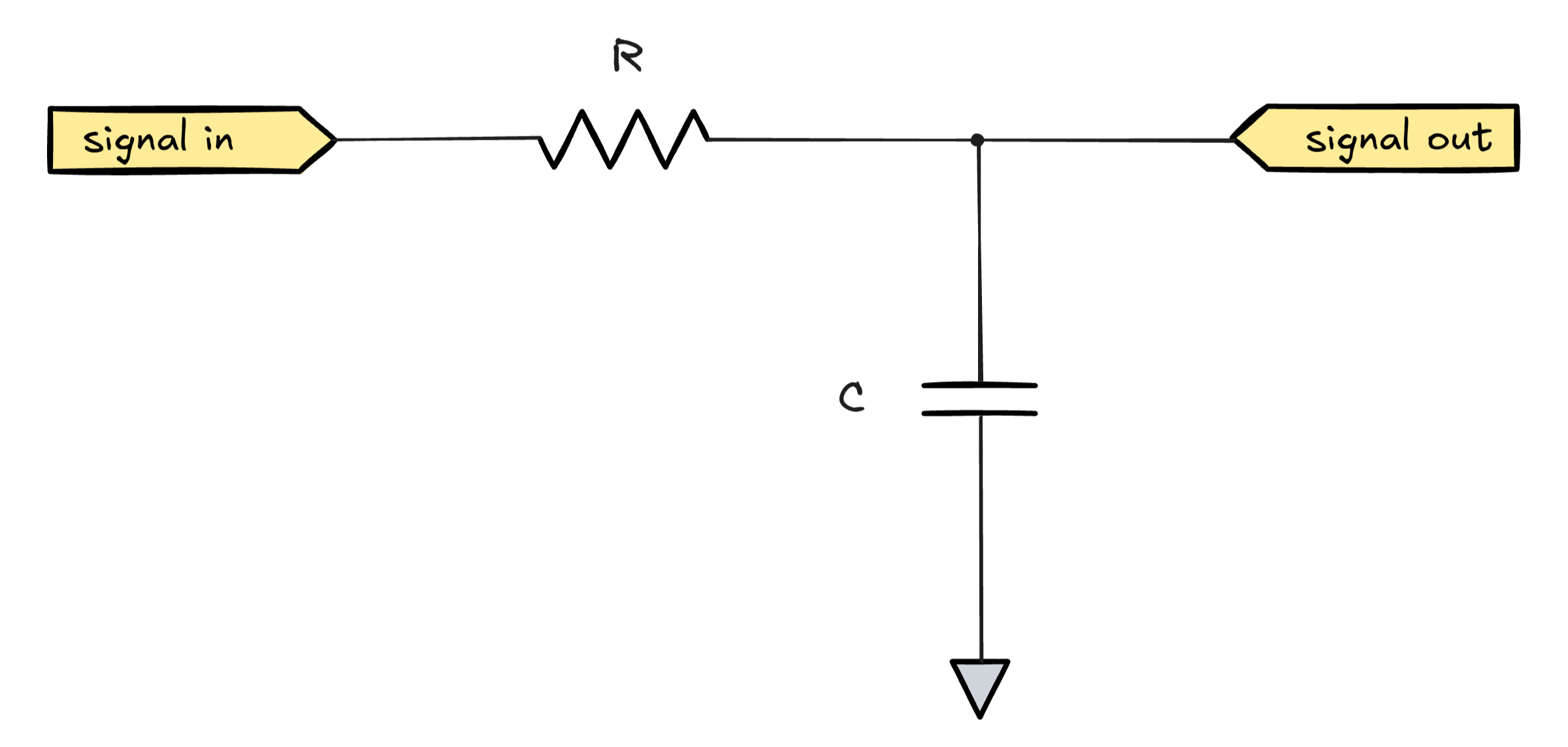
The filter can be thought of as a voltage divider in which R is constant and C begins to conduct better as the sine-wave frequency of the input signal increases. This frequency-dependent resistor-like behavior of a capacitor is known as reactance and is described by the following formula:
Most sources give this equation without explaining where it comes from, but it can be derived with basic trigonometry; if you’re unfamiliar with its origins, you might enjoy this foundational article posted here back in 2023.
In an R-C lowpass circuit, the reactance is initially much larger than the value of R, so up to a certain frequency, the capacitor can be ignored and the input voltage is more or less equal to the output voltage. Past a certain point, however, the reactance of the capacitor becomes low enough so that the signal is markedly pulled toward the ground, attenuating it and producing a filter response plot similar to the following:

It’s easy to find the frequency at which R = XC. The solution corresponds to the “knee” in the logarithmic plot shown before:
This is basic analog electronics, and something we covered on the blog before. But did you know that you can construct a perfectly good lowpass filter with a pair of capacitors and a toggle switch? The architecture is shown below:
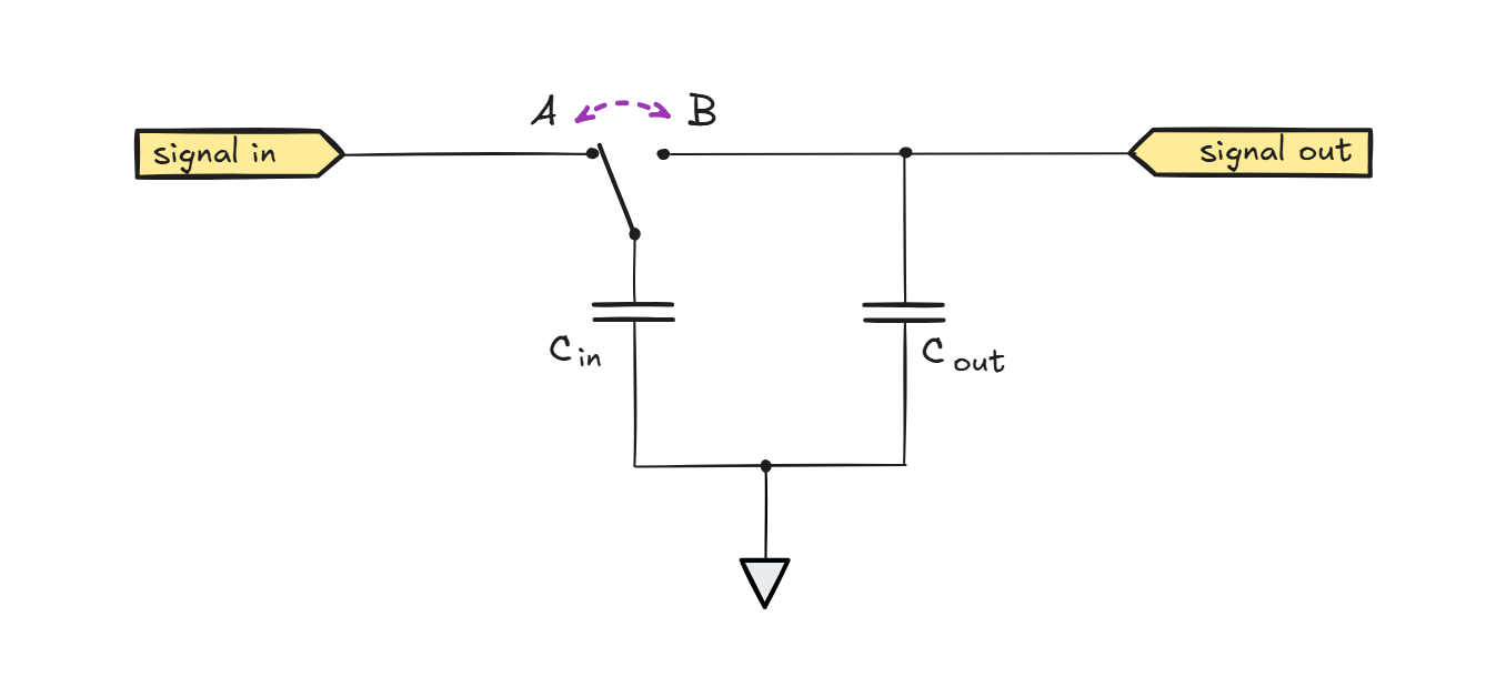
In practical circuits, the “switch” would be a pair of MOSFETs driven by a timing signal, but nothing stops us from using a real switch or an electromechanical relay to experiment with this topology on a breadboard.
In the first half of the timing cycle, the switch is in position A. This connects a small input capacitor, Cin, to the input terminal. As soon as the connection is made, the capacitor charges to a voltage equal to the momentary level of the input waveform, which we can denote as VA.
In the second half of the cycle, the two-way switch is moved to position B. This causes the voltages across Cin and Cout to equalize. We don’t need to solve for the relative shifts in their terminal voltages; it suffices to say that Cin started at VA and ended up at VB.
With this in mind, we can apply a a form of the fundamental capacitor equation (I = C·Δv/t) to find the average current that must have flowed out of Cin to shift its voltage by that amount in time t:
The switching period t is the reciprocal of the switching frequency fs, so we can also restate this as IB = (VA - VB) · Cin · fs.
The formulas tell us that the average current is proportional to to the voltage present across the A and B terminals of the switch. The actual current is pulsed, but it otherwise looks like the ohmic behavior of a series resistor. In fact, from Ohm’s law, we can find the equivalent resistance that appears to be feeding Cout:
If the circuit can be modeled as a series resistor feeding a shunt capacitor, we’re essentially looking at a bog-standard lowpass R-C architecture. The knee frequency of this R-C filter can be written as:
The math might seem improbable, but the circuit works in practice. The following oscilloscope traces show a filter constructed with Cin = 100 nF and Cout = 1 µF, toggled at fs = 50 Hz. This corresponds to fknee ≈ 0.8 Hz — and indeed, we see some attenuation for a 1 Hz input sine, and a lot more for a 5 Hz one:
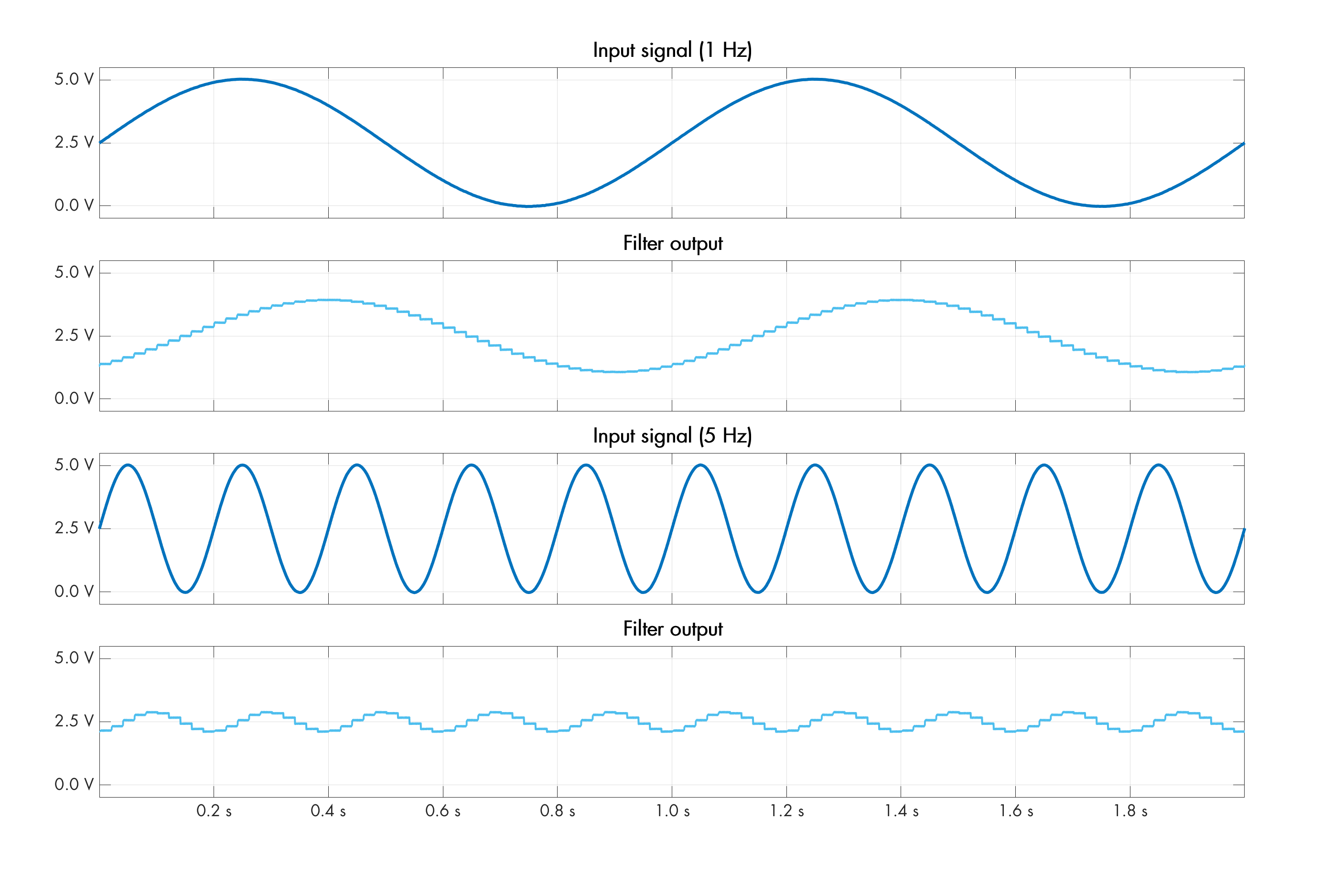
The plot also offers an intuitive interpretation of the math: in each clock cycle, only a certain amount of charge can move between the capacitors; this corresponds to the maximum height of a single step in the output waveform, proportional to the relative sizing of the caps (i.e., the ratio of Cin to Cout). The larger the vertical step, the easier it is for the output waveform to track a fast-moving input signal.
The switching frequency fs controls how many charge transfers occur per second, which gives us another method of controlling the filter’s center frequency: to shift it, we can speed up or slow down the supplied clock. That’s a major boon for digitally-controlled analog signal processing.
In practice, to minimize the stairstep pattern, we tend choose the switching frequency fs to be about two orders of magnitude higher than the filter’s intended center frequency. To achieve this, from the earlier fknee formula, we need to aim for Cout ≈ 16 · Cin.
And, to answer the obvious question - yes, it's used in practice. For example, you can buy high-order IC-based filters that give you a very steep frequency rolloff (e.g., close to that ideal "brick wall" response) and where you select the center frequency by supplying a clock.
https://www.analog.com/media/en/technical-documentation/data-sheets/max291-max296.pdf