How do transistors work, anyway?
The internet is littered with explanations of how transistors work. Most of them don't really explain anything.
The invention of the electronic circuit changed the world. In just over a century, electronic devices upended almost every aspect of our lives — from transportation, to medicine, to the way we interact with each other and have fun.
Despite this, a firm grasp of electronics remains elusive for most. I’m confident that much of the blame lies with the hydraulic analogy — a reimagining of electronic circuits as series of tubes. The hydraulic analogy is seductive to textbook authors but quickly spring leaks. By the time you get to transistors, you’re constructing bizarre two-stage water valves that don’t truly emulate semiconductors — and would give your plumber a headache, too.
Indeed, the mechanics of transistors remain mystifying to most hobbyists, making it hard to comprehend the design of fundamental devices such as operational amplifiers. In this post, I’m hoping to shed some light on the topic — hopefully without bringing up quantum wave functions, but also without reaching for a pipe wrench.
The physics of conduction
Let’s start with a refresher on the physics of conduction. In solid-state electronics, the flow of electricity can be explained by the motion of outer (valence) electrons that skate across stationary atoms or molecules.
In most materials, valence electrons are not particularly mobile and a considerable energy is needed to push them around; that energy is often sufficient to set things on fire along the way. This situation is different in metals, where valence shells are mostly empty and the atoms are packed very densely, so some electrons at their normal energy levels can freely move from one atom to another. These mobile electrons form what’s known as an electron gas.
The attraction to positively-charged protons confines the electrons to the bulk of the conductor. The electrostatic repulsion between electrons, on the other hand, generally compels them to spread as far as possible, filling the entirety of the available space.
It should be underscored that the flow of electricity has less to do with the travels of individual electrons, and more with what can be thought of as pressure equalization in this electron gas, mediated through electromagnetic fields. In a typical circuit, the drift of an electron averages millimeters or centimeters per hour. Yet, shoving an extra electron onto a metal wire causes nearby ones to scuttle away without coming into contact with each other — a cascading wave that propagates at close to the speed of light.
Such electromagnetic forces can also act across non-conductive gaps; for example, bringing an negatively-charged rod near one end of a metal wire will cause some electrons in the conductor to scamper away toward the other side.
The two most important concepts in electric circuits are voltage and current. Current is a straightforward measurement of the number of electrons traveling through a particular spot in a unit of time. Voltage, on the other hand, can be thought of as a measure of a pressure differential in the electron gas. Simplifying a bit, the higher the difference between two chosen points, the higher might be the current that flows if you accidentally drop your plumbing wrench across that portion of the printed circuit board.
Note: if this abridged explanation feels unsatisfying, check out this primer on electricity and a second article with a more detailed explanation of voltage and current.
The case of semiconductors
There is an intermediate class of materials, known as semiconductors, where the outer electrons are nominally immobile, but where only a slight nudge is needed to knock them into a higher-energy state and set them free. This nudging continually happens on its own due to random, room-temperature thermal events.
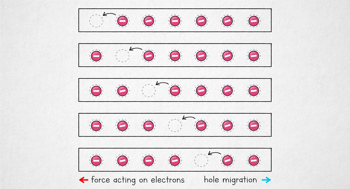
In semiconductors, these excited electrons soon return to a lower energy state; but in the presence of an external electric field, they might be able to drift a short distance. The slack they leave behind in the valence band also allows some lower-energy electrons to slither around.
Although it might sound goofy, it’s equally valid to visualize the process as the motion of electrons, or as the drift of valence shell vacancies (“holes”) in the direction opposite to where the electrons are trying to go:
Either way, this stop-and-go process allows a (rather weak) current to flow.
Pure semiconductors have poor electrical properties because the number mobile charge carriers is low, but the material’s conductivity improves significantly in the presence of impurities known as dopants. An n-type dopant, such as phosphorus, adds some mobile (conduction band) electrons that don’t have low-energy vacancies to return to, in effect increasing the number of charge carriers available at any given time. Conversely, a p-type dopant, such as boron, contributes valence shell vacancies in the base material that are not paired to any momentarily-excited electron.
The improvement in the conductivity of n-doped materials is fairly easy to grasp: there’s more long-lived, mobile electrons that can respond to applied fields. The mechanism in p-doped semiconductors is a tad more nuanced: the slack afforded by long-lived holes means that the distribution of non-excited valence electrons can all of sudden shift with more ease in response to external electric fields, with no need for the charge carrier to be thermally excited into the conduction band.
Again, you can think of this as electrons opportunistically slithering into nearby vacancies, or you can look at holes as weird, disembodied “particles” that drift in the opposite direction in a sea of valence electrons. However you approach it, both n-type and p-type materials conduct much better than pure silicon.
It should be noted that doped semiconductors remain electrically neutral. Only the distribution of electrons at different energy levels is changing, not the ratio of electrons to protons in the crystal lattice.
Semiconductor junctions
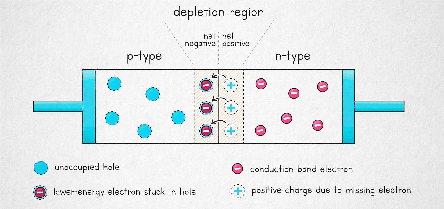
When a p-doped semiconductor is brought into contact with an n-doped one, an interesting phenomenon takes place: within an exceedingly thin layer, free electrons from the n-side diffuse across the boundary and promptly fall into the immediately adjacent, abundant valence holes present on the p-side:
This creates a depletion region: a layer that has virtually all the holes plugged on the p-side, and practically no excited, conduction-band electrons on the n-side. Internally, the region is no longer electrically neutral, with a concentration of negative charges on the p-side (due to surplus electrons) and positive charges on the n-side (due to all the orphaned, electron-deficient atoms still stuck in place).
This produces an internal electrostatic field within the junction, pushing electrons from left to right. The field prevents the passage of majority charge carriers: if any electron wanders in from the n-side, or any hole wanders in from the p-side, they’re expelled back to where they belong. It is still possible for minority carriers to cross — for example, the odd mobile electron that wanders in from the p-side will be accelerated to the n-side — but because of the low density of such charge carriers, the effect is more or less negligible.
From the diagram, it should be clear that removing electrons from the right terminal of the device and adding them to the left terminal does not accomplish much. The action adds to the existing electric field and widens the depletion region. Reverse breakdown can happen at a sufficiently high voltage, for example if charge carriers are accelerated to the point of knocking electrons into the conduction band in an avalanche-like effect. That said, in a standard diode, this voltage is kept well outside the component’s intended operating range.
Moving the electrons in the other direction is another story. It gradually counters the junction’s internal field, eventually getting the p-side electrons unstuck and allowing more n-side electrons to cross. For silicon devices, the voltage needed to get things going hovers around 600 mV. Past that point, the junction (known as a diode) becomes an excellent conductor — that is, until the applied voltage drops below that magic threshold again.
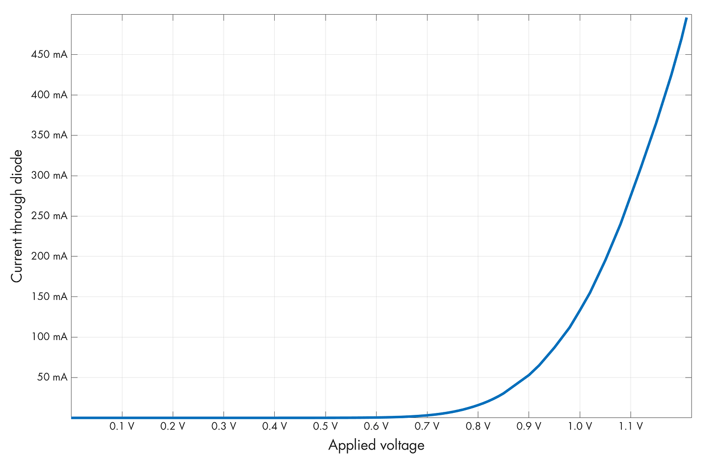
Some sources describe the diode’s V-I curve as exponential, but this is not true for real-world components. At first, the current does follow that pattern; but before long, the inherent resistance of the material starts to dominate and the relationship between current and the “excess” voltage becomes roughly linear.
Because of the ~600 mV conduction threshold, the junction is sometimes described as having a “built-in voltage”, but this is language is imprecise. Voltage is a concept that measures the force compelling electrons to move from one point to another to reach a thermodynamic equilibrium. In the case of a p-n junction, there equilibrium is the lopsided distribution of charges. If you connect a voltmeter to the junction, it will show 0 V.
Junction field effect transistors (JFETs)
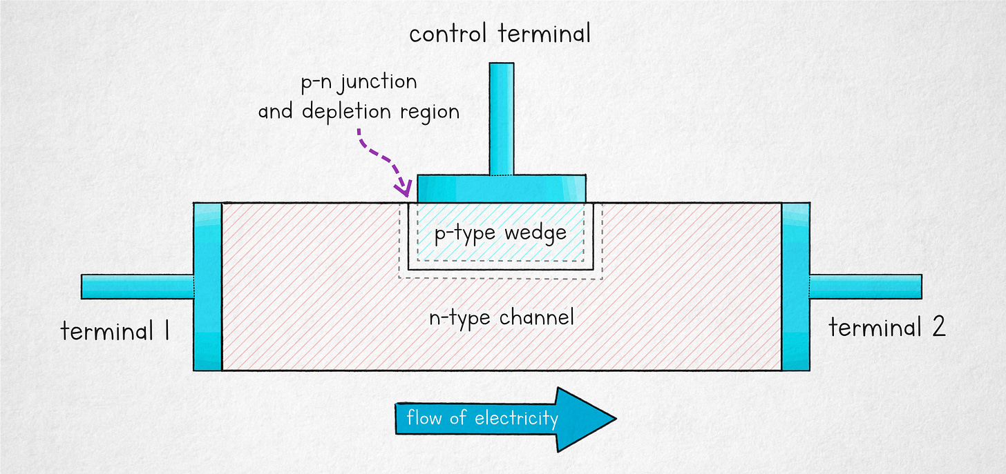
A simple p-n junction may seem uninteresting, but it’s a versatile building block. To illustrate, let’s start with junction field effect transistors that use a reverse-biased p-n junction as a way to moderate the current flowing between their two primary terminals — drain and source:
There are no semiconductor junctions between the two primary terminals. You can find a p-n junction near the control terminal — the gate — but it’s never meant to conduct, and it is kept below 600 mV.
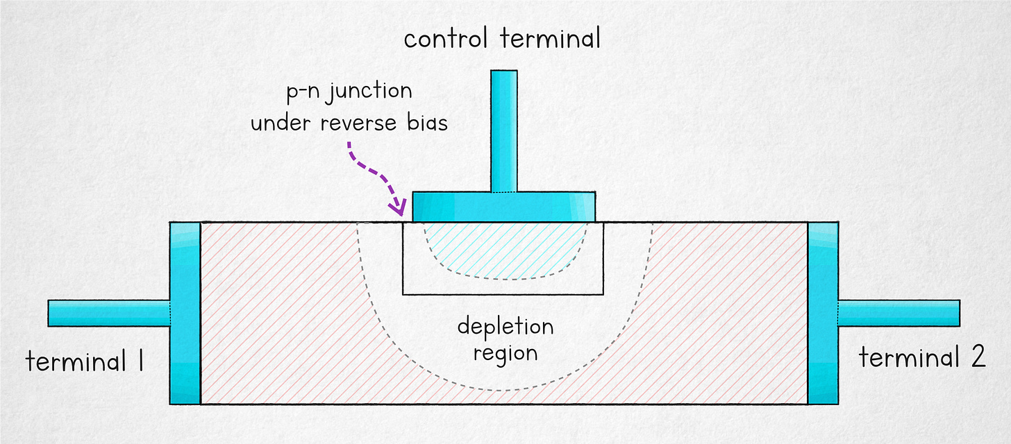
When the gate voltage is around 0 V relative to the n-region, the depletion layer is present but very thin, so it doesn’t impede the flow of current between the source and the drain. But as the voltage is lowered, the junction becomes reverse-biased, the depletion region expands, and the effective width of the channel shrinks. By the time you get to perhaps -5 V, it grows so large that it pinches off the conductive path through the n-doped body of the device:
JFETs are remarkable because they respond stoutly (and rather linearly) to small voltages applied to the gate, making them well-suited for building amplifiers:
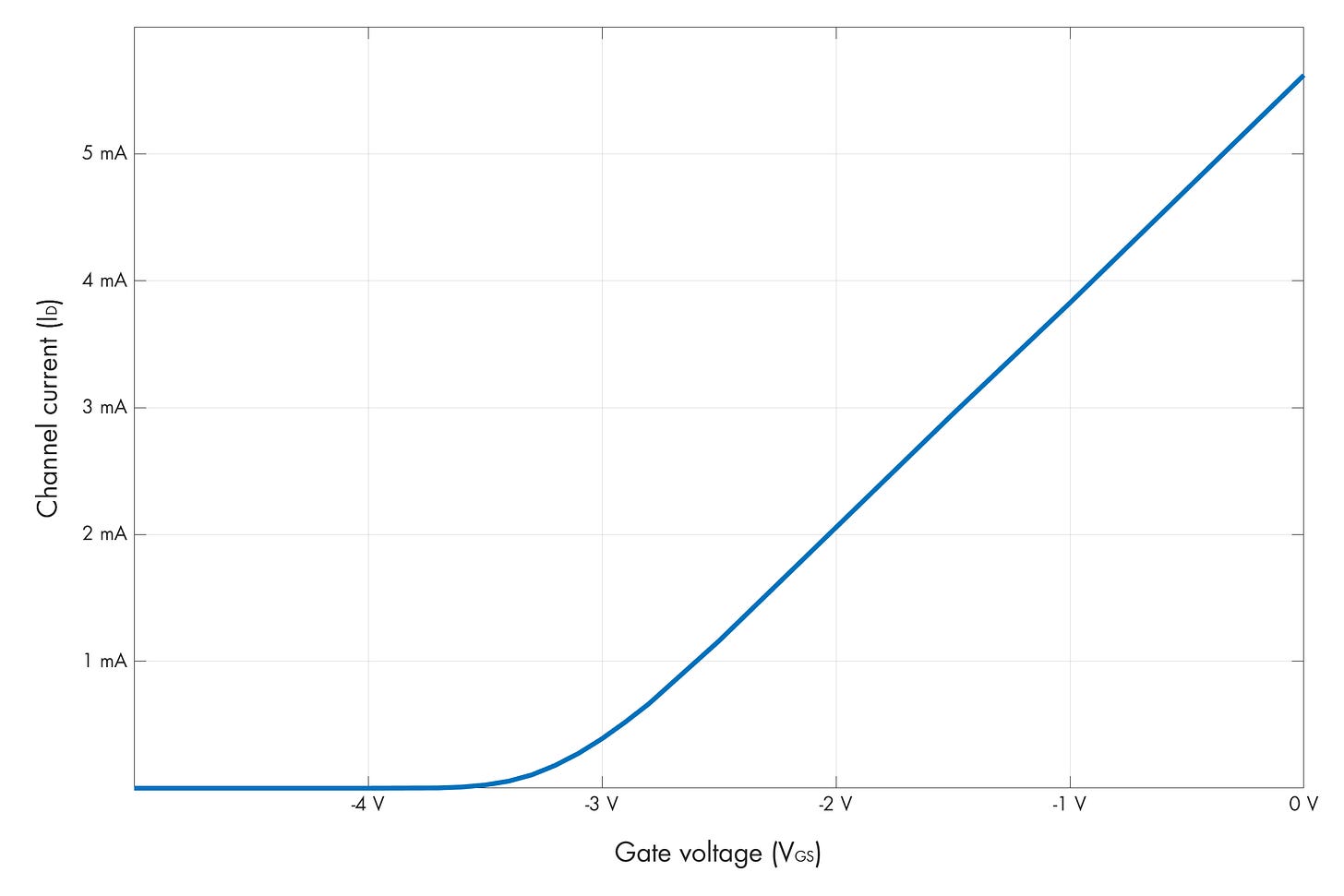
Despite these desirable characteristics, these transistors have been largely replaced by another design with a higher current capacity: the MOSFET.
Metal-oxide-semiconductor field effect transistors (MOSFETs)
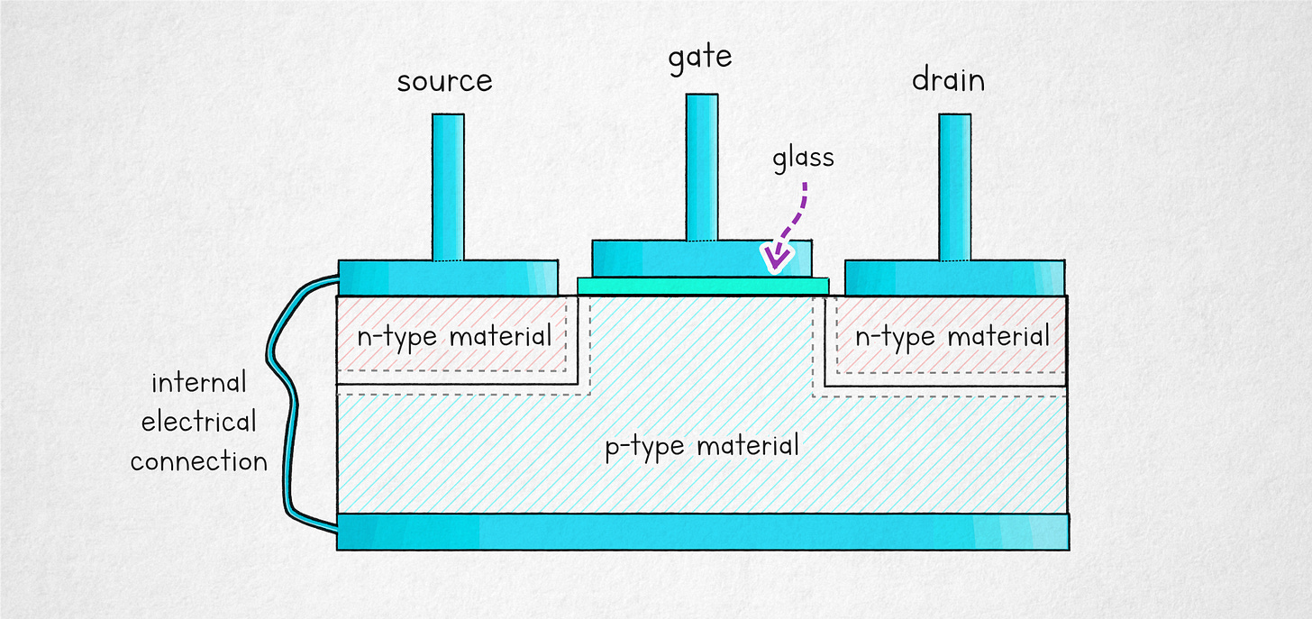
Much like JFETs, MOSFETs are designed to control the flow of current between their two primary terminals — source and drain — via a variable voltage applied to the gate. That said, their internal architecture is a bit more complex:
The drawing shows an n-p-n junction in the path of the current; because one half of this junction is inevitably reverse-biased, it would appear that the transistor should never conduct.
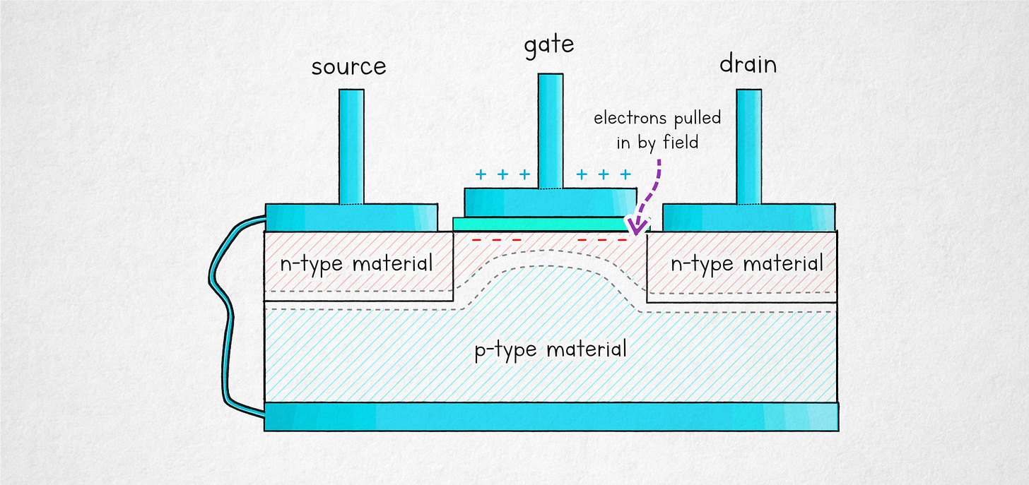
Of course, MOSFETs have a trick up their sleeve: if a sufficiently high positive voltage is applied to the insulated gate (relative to the “substrate” terminal), the resulting electric field pushes away holes in the p-type material on the other side of the insulator and attracts minority-carrier electrons, forming an n-like inversion layer. This electron-rich channel eventually bridges the source and the drain:
The marvelous property of MOSFETs is that no electrical connection is needed between the gate and the rest of the device. The nearly-perfect isolation of the input signal makes them remarkably efficient (with a caveat about capacitance, discussed later on).
In theory, MOSFETs could be operated with no special regard to the polarity of their two primary terminals. In practice, most discrete MOSFETs come with the substrate internally tied to the source, as shown in the illustration above. This is done to improve the capacitive properties of the gate, allowing more charge to move in and out without the need for high driving voltages. The connection turns the transistor into a device that, in its “off” state, behaves like a reverse-biased diode when hooked up correctly, and starts unexpectedly conducting in a forward-bias condition (i.e., when the source and drain polarity is incorrect).
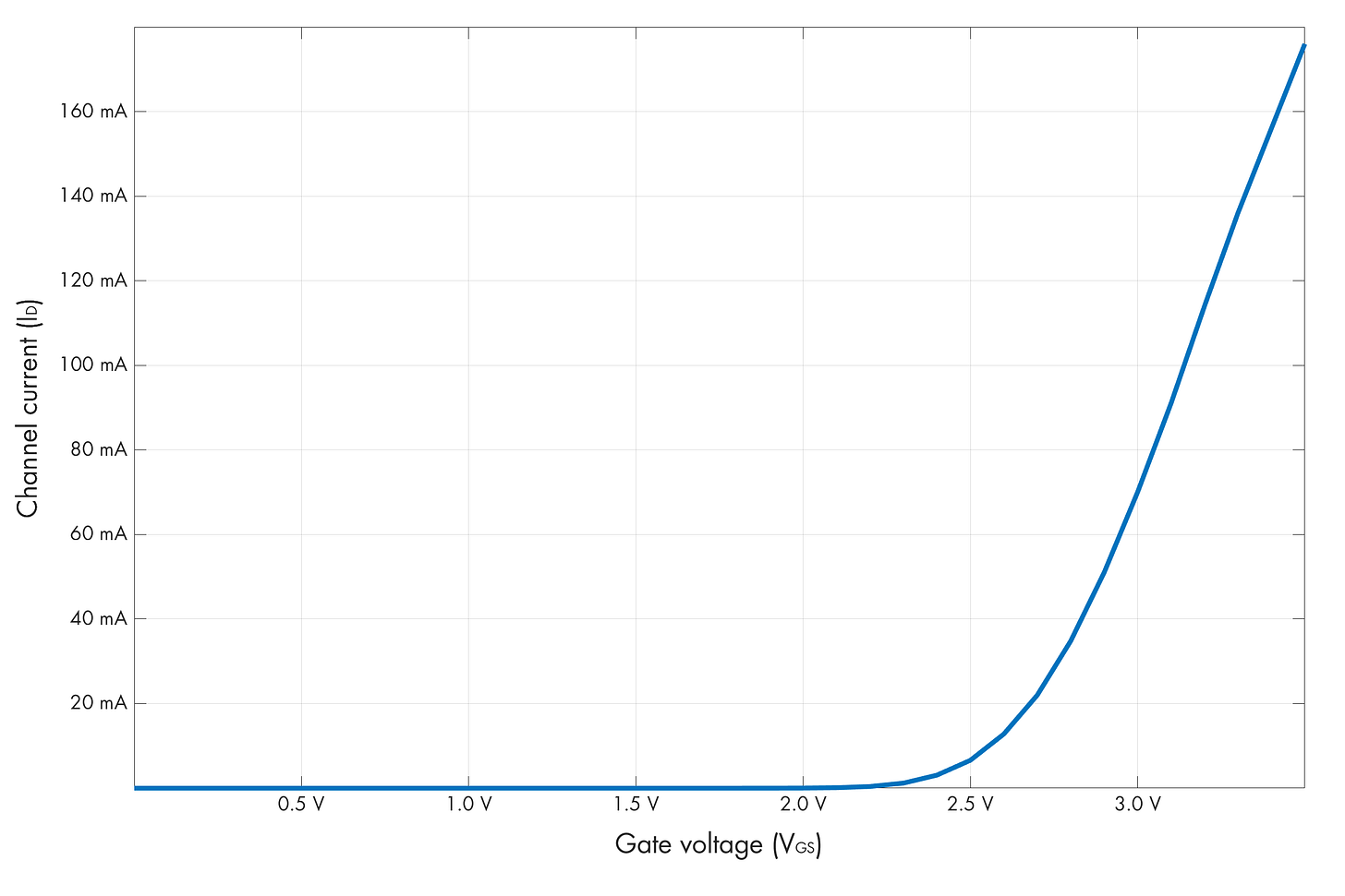
MOSFETs are the workhorses of the semiconductor industry. Their main drawback is that it takes a substantial gate voltage to get them going; about 2 V is common for discrete transistors, and as much as 10 V might be necessary to reach the “fully on” state needed to efficiently drive higher-current loads. Compared to JFETs, the required threshold voltage complicates certain signal amplification tasks:
Another gotcha of MOSFETs is that there is a substantial capacitance between the gate and the substrate: after all, you have two conductive layers separated by an exceedingly thin insulator, resulting in a structure that resembles a standard capacitor. In discrete transistors, the capacitance usually ranges from 10 pF to 1 nF. The value, if not accounted for properly, can cause energy losses, slow rise and fall times, or unwanted signal coupling if the signal supplied to the gate has a sufficiently high frequency.
Bipolar junction transistors (BJTs)
Some readers might be wondering why I didn’t begin with the bipolar junction transistor. The answer is simple: the venerable BJT is the oldest truly successful transistor design, but it’s also the messiest of the bunch.
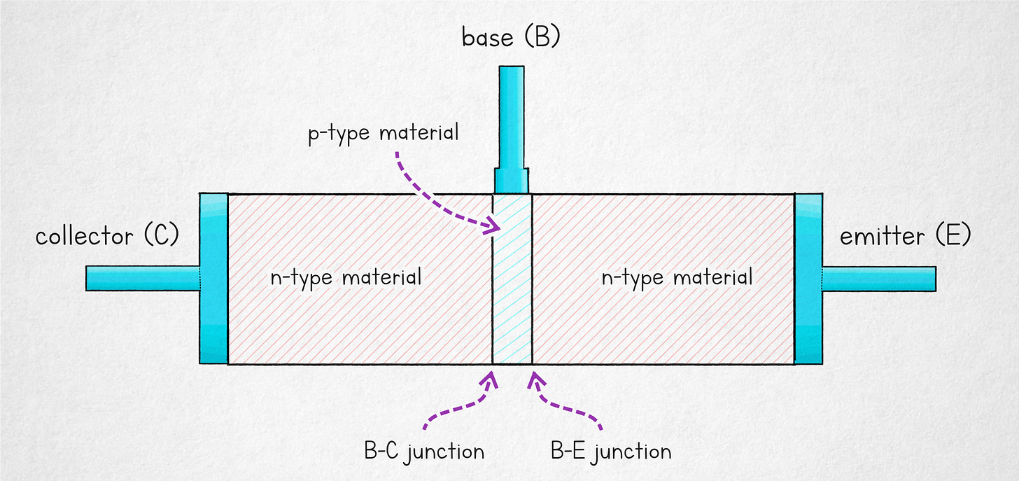
Let’s have a look at the common n-p-n layout. Similarly to a MOSFET, the double junction between its main terminals — the collector and the emitter — is nominally non-conductive because one half of it is reverse-biased. Of course, at this point, you should be expecting a hat trick. The BJT trick is that the middle layer is made extremely thin, often around 1 µm; this places p-side depletion regions right next to each other.
With this detail out of the way, let’s start with the obvious: if you apply a sufficient positive voltage to the control (base) terminal in relation to the emitter, you can overcome the internal electric field of the base-emitter (B-E) junction and cause electrons from the emitter region to start pouring into the base layer. Similarly to a standard silicon diode, this happens around 600 mV.
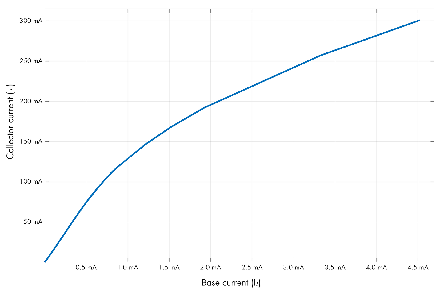
The electrons are notionally supposed to recombine with holes in the base region, but because the layer is so thin, they can also easily diffuse into the immediately-adjacent base-collector depletion region. In there, because they’re wandering into it from the “wrong” side — from the p-region where electrons are the minority charge carriers — the internal field of the B-C depletion region whisks them away toward the collector terminal, causing an unexpected “side” current to flow. In fact, in a properly-designed BJT, a relatively small base current can trigger a considerably higher current in the C-E path. There is a sorta-linear relationship between the two currents:
The idealized drawing of a BJT might imply that it should be a bidirectional device, working equally well if you reverse the polarity of the collector and the emitter. In practice, the emitter region is usually doped more heavily to facilitate the transport of electrons in one direction; in other words, reversing the component is possible, but its performance will be poor.
There are two things that make BJTs messier than FETs. First, they’re current-controlled, which is typically less convenient than voltage control. Second, the B-C junction on the left needs to be watched too: if the collector voltage becomes lower than the base voltage (~600 mV), the B-C diode becomes forward-biased, and some of the control current is diverted down that path. If this happens, further increases to IB have a diminished effect on IC. This means that the transistor can’t be “opened up” as fully as a FET, and there’s some inevitable collector-emitter voltage drop.
📖
If you liked the article, you’ll enjoy The Secret Life of Circuits. It’s a richly illustrated, lucid introduction to electronics — from the physics of conduction to embedded system programming. It features 290+ color diagrams, 420+ pages of original content, and zero AI.
👉 For other articles about electronics, click here. In particular, you might like:
I write well-researched, original articles about geek culture, electronic circuit design, algorithms, and more. If you like the content, please subscribe.






One of the most important part is two paragraphs between "From the diagram, it should be clear..." and "...if the current flowing through it isn’t limited in some way."
I've majored in physics, particularly electronics, but I still need to stop and think carefully, in steps, what those two paragraphs explain and why. I guess a bit more detailed explanation and maybe a picture could help.
Brilliant explanation. A follow-up discussion on transistor biasing would be perfect!