The basics of signal amplification
Single transistors to push-pull amplifiers to op-amp chips: what is "signal amplification" and how to get it right?
As a computer geek, I never had much trouble navigating the world of microcontrollers and logic gates. Analog circuitry proved to be a different story; for a good while, I resigned myself to copying other people’s designs and going on wild-goose chases to procure long-obsolete parts that cropped up on the schematics.
After years of experimentation and study, I can navigate the world of analog signals with reasonable ease. In today’s article, I’d like to share some notes on one of the most common circuit design tasks: amplifying weak signals to make them suitable for driving analog-to-digital converters, speakers, LEDs, and other I/O devices.
Note: this article assumes a solid grasp of voltage, current, resistance, and how they relate to each other. If you need a refresher, start here.
What is amplification, anyway?
There are two types of amplification circuits you are most likely to encounter: voltage and power amplifiers.
Voltage is straightforward. Voltage levels are the primary way of conveying information in electronic circuits, and every now and then, you encounter signal amplitudes that are too small for the intended purpose. An example might be the output of an electret microphone, a photodiode, or a temperature sensor — all firmly in the millivolt range. The job of a voltage amplifier is to multiply the voltages by some fixed value (“gain”), thus producing an output signal suitable for your needs.
Power amplification is different. You might have come across a signal that looks good on an oscilloscope screen, but drops precipitously when connected to a load; a classic example is a microcontroller output pin interfaced directly to a motor or a speaker. The signal’s sudden attenuation is a straightforward consequence of Ohm’s law: V = IR. A single pin on an MCU has a limited current capacity, typically no more than 40 mA; if the connected load sinks more than the chip can supply, the voltage must sag. For instance, if we’re driving an 8 Ω speaker, the voltage across the speaker’s terminals will not exceed 320 mV (40 mA * 8 Ω), no matter what the chip is hoping to achieve.
A source that can’t supply appreciable currents is said to have high impedance. A power amplifier is a device that takes this high-impedance signal and then cranks out a low-impedance copy through a beefy output stage that can supply larger currents with ease.
Conditioning signals for amplification
A near-universal constraint of amplifier circuits is that they can’t output voltages higher than the positive supply rail, or lower than the negative one. The output range is sometimes more constrained, but almost never extends beyond the supply.
It follows that if you have a signal that fluctuates between 1.0 and 1.05 V, and want to obtain a 5 V output swing, you can’t simply amplify it by a factor of 100 in relation to the ground; that would put the output in the out-of-whack range of 100 to 105 volts. It can be similarly challenging to amplify any signal that extends below the negative supply rail, as some audio signals are liable to:
Short of building a second, wider-range voltage supply just for the amplifier, the most obvious solution is to offset the signal before amplification. Let’s go with an example of an input waveform centered at 0 V and exhibiting a peak-to-peak amplitude of 5 volts. We can use the following circuit to pull it up:
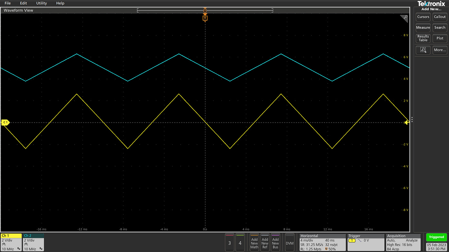
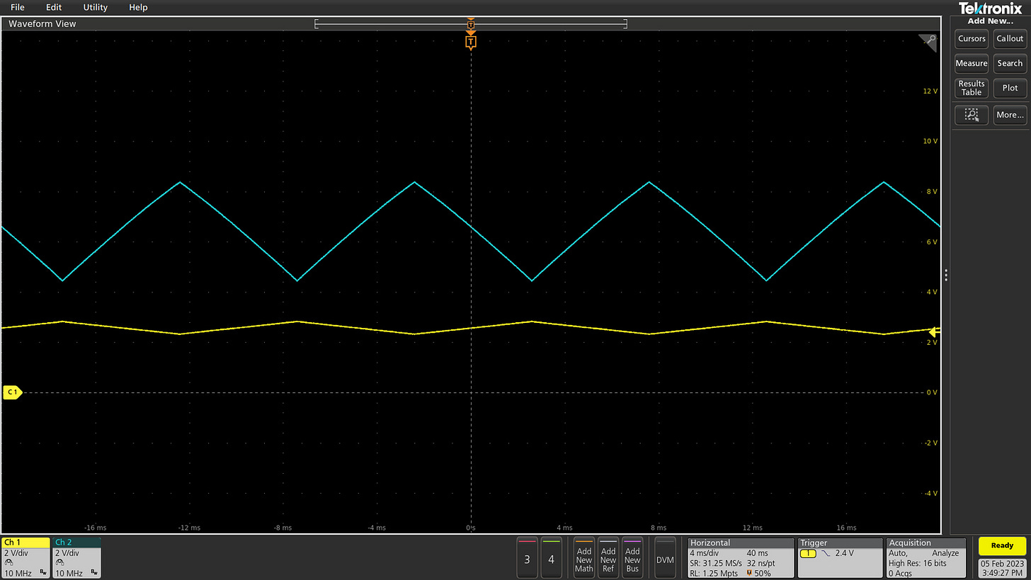
For the sake of this thought experiment, let’s use the same value of R1 and R2, perhaps 10 kΩ. In this case, the output should be a simple average, with 50% contributed via the R1 leg, and 50% contributed from the +10 V rail via R2. If so, one would expect the new signal center point to be the average of the center points of the two input components: (0 V + 10 V) / 2 = 5 V. In the same vein, the new peak-to-peak amplitude should measure (5 V + 0 V) / 2 = 2.5 V.
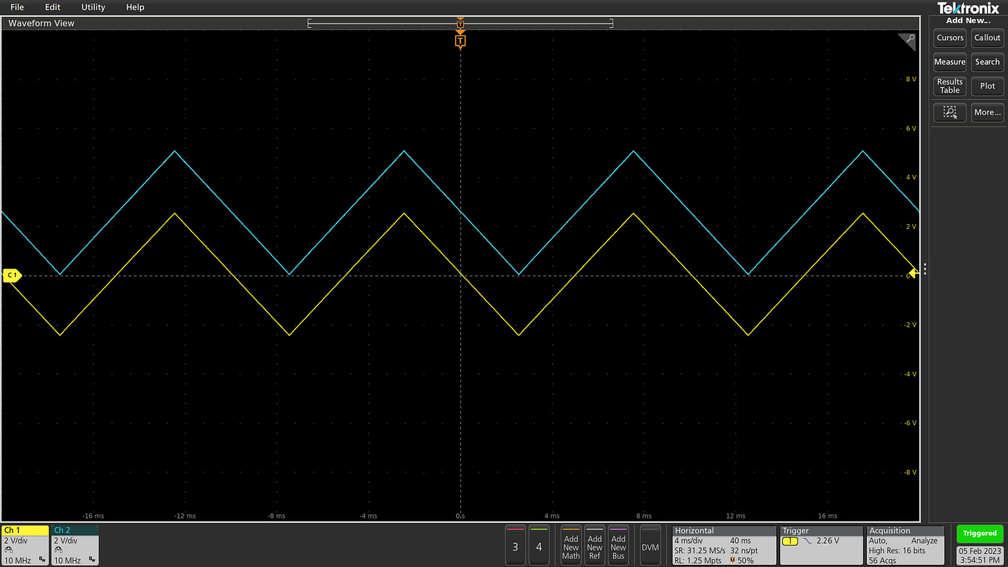
A quick test with an oscilloscope confirms the calculations. The original signal is shown in yellow, while the offset version is in blue:
Other ratios are possible; had we used R1 = 10 kΩ and R2 = 33 kΩ, we’d have ended up with a center point at ~2.3 V and a peak-to-peak amplitude of ~3.8 V. The only practical constraint is that the input resistor — R1 — must be kept large enough to avoid loading the source to any appreciable extent.
The most obvious problem with this circuit is that although it succeeds at offsetting the signal, it inevitably reduces its amplitude. This can be compensated for by increasing amplifier gain down the line, but extra noise is the price to pay for such shenanigans.
A more elegant solution is possible if we don’t care about preserving DC voltages, only about any higher-frequency AC signals that might be riding on top. This is common in audio circuits, and in this scenario, we can employ a DC-blocking capacitor in the signal path:
If the impedance of R1 and R2 is much higher than the impedance of C at a particular signal frequency, then from the perspective of that signal, we can consider one of the capacitor legs to be free-floating. This precludes the capacitor from charging or discharging in response to sufficiently fast input voltage swings; instead, its charge state remains constant and the component just serves as a conduit for electromotive force: an AC voltage applied on the input leg of the circuit produces an equivalent, sympathetic electromotive force on the other leg.
At the same time, in a lower-frequency view, the impedance of C increases, and at some point, it approaches the impedance of R1 and R2. At that point, the current flowing through the resistors is no longer negligible, allowing the capacitor to slowly build up some internal voltage. In particular, if R1 = R2 and the input sine has an average voltage of zero, the capacitor will charge to Vcap = Vsupply / 2. This voltage then adds to the fast-changing AC waveform.
It follows that the circuit can be used to shift AC signals to a chosen midpoint with virtually no change in amplitude at higher frequencies:
What are these “higher frequencies”? Well, assuming that there is no substantial output loading, the circuit’s frequency response characteristics are dictated chiefly by the RC highpass filter formed by C and the output-side resistors. If R1 = R2, the filter’s cutoff frequency is: f = ¼ × π × R1 × C.
As a practical example, with a 100 nF capacitor and two 100 kΩ output resistors, the the amplitude would start to roll off noticeably around 8 Hz.
Transistors as voltage amplifiers
This chapter assumes familiarity with the behavior of transistors, especially MOSFETs; if you need to jog your memory, please refer to this earlier article.
A transistor’s simplest use is as a switch. Let’s consider a common n-channel MOSFET in the following arrangement:
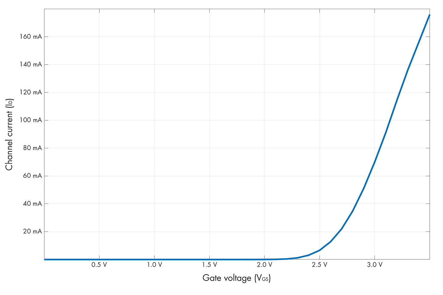
This transistor remains non-conductive until the Vgs voltage — the difference between its control terminal (gate) and its low-side terminal (source) — exceeds the transistor’s intrinsic threshold. The threshold voltage (Vth) usually hovers around 2 V, but varies from one transistor to another. Once Vgs clears Vth, the device starts conducting (at first only slightly), and the load is energized.
There is a small linear region between “fully off” and “fully on”, and in this region, the transistor exhibits variable resistance proportional, among other things, to the applied gate voltage. Knowing this, many novices attempt to amplifiers by extending the switch topology, like so:
In this layout, we have a fixed resistor (R) in series with a variable resistance that changes dramatically in response to small swings of the input voltage; at the midpoint of this voltage divider, we should see an amplified version of the input signal.
This design sort-of works, is usually a mistake: the transistor’s voltage gain in that quasi-linear region is very high but unpredictable; it varies from batch to batch, and is affected by factors other than Vgs. To build a dependable amplifier, it is typically necessary to incorporate a feedback mechanism of some sort. A wider operating range would be nice too!
Building a voltage follower
Recall that an n-channel MOSFET begins to conduct to an appreciable extent only when Vgs > Vth. In the previous example, we had the source terminal tied to the ground, so the Vgs swing was always equal to the magnitude of the input signal (Vsignal). But what if we allowed the source leg to drift away from 0 V?
To analyze this circuit, let’s suppose that R = 10 kΩ, that the transistor’s threshold voltage is 2 V, and that a 5 V signal is supplied on the input terminal.
At first, the source terminal is at ground potential, so Vgs is equal 5 V and the transistor becomes conductive. Soon thereafter, in response to the flowing current, a voltage develops across the resistor (V = IR), dragging the source terminal to a higher potential. By the time the current reaches 300 µA, the source leg is at 3 V (10 kΩ * 300 µA), so Vgs is effectively reduced to 2 V. This is the threshold voltage of the transistor; any further increases in the current would cause it to shut off. We reach a equilibrium: Vout ≈ Vsignal - Vth.
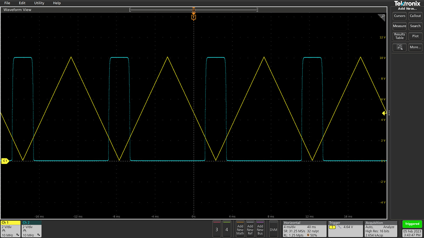
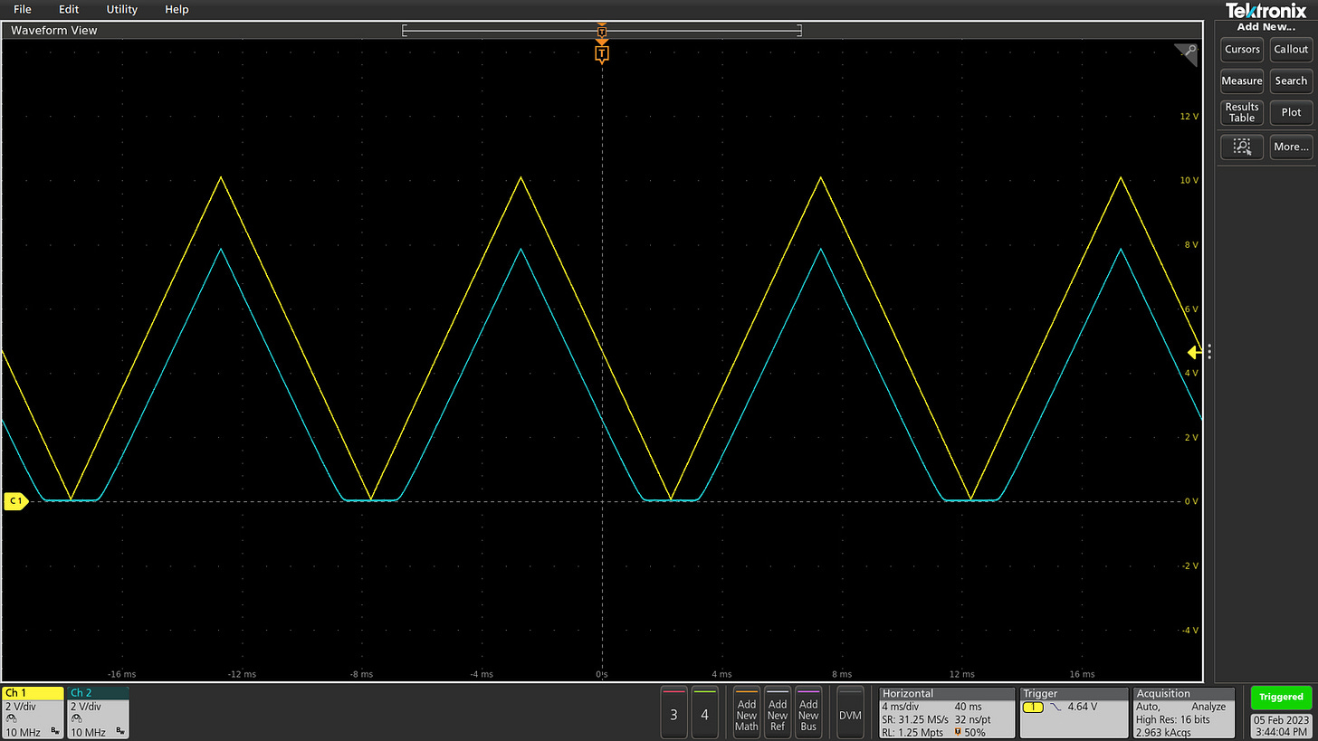
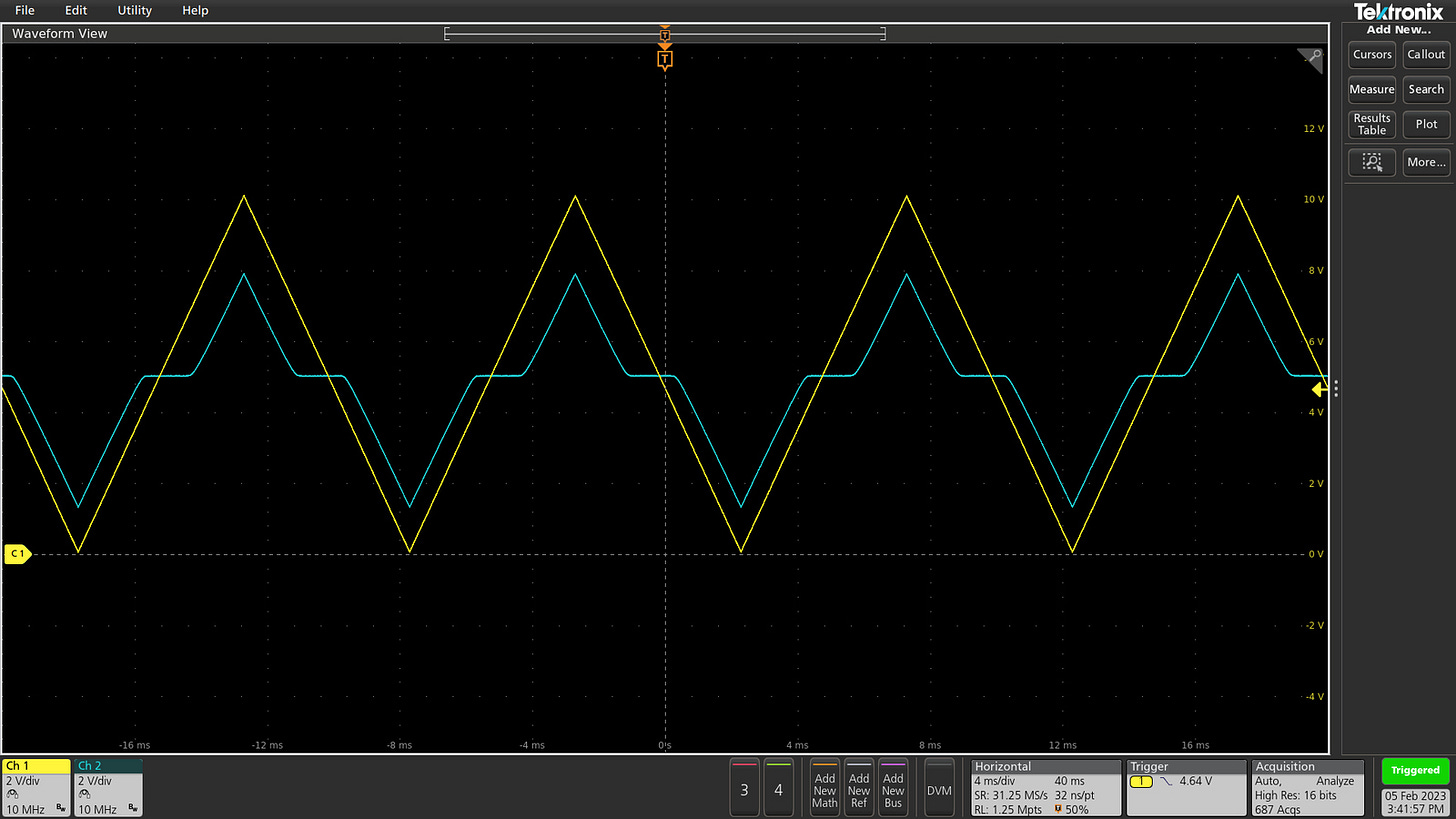
The following oscilloscope plot shows the behavior of the circuit; the input signal is shown in yellow, while the output is blue:
Of course, the circuit isn’t a voltage amplifier, but it is a building block for one. It does offer power gain if R is replaced with a real load, although its drive capabilities are asymmetric: if you connect a capacitor between the output terminal and the ground, the circuit will only be able to charge it to higher voltages as the input signal rises, not discharge it back when the input signal falls and the transistor cuts off.
The oscilloscope plot shows an expected, Vth-related offset between the input and the output signal; because the circuit can’t output voltages lower than the ground, some of the shifted waveform is also clipped at 0 V. To avoid such distortion, one would need to gently offset the input signal beforehand.
Toward a voltage amplifier
Let’s make a small modification to the voltage follower circuit by adding a second resistor on the high side of the MOSFET:
For a moment, let’s assume that R1 = R2. The fundamental feedback mechanism of the circuit remains the same as before: the transistor will admit current sufficient to create a self-limiting feedback voltage across R2. This equilibrium voltage is always Vsignal - Vth. But because the same current is necessarily also flowing through the newly-added R1, the extra resistor will develop a voltage drop across its terminals, too. If the resistances are the same, the drops will be of equal magnitude.
This may seem uninteresting, but now consider what happens if R1 is larger than R2. The current through the circuit is set by the R2 feedback mechanism; as for R1, from Ohm’s law, we know that if the current stays the same but the resistance increases, we should see a proportionately larger voltage drop on that side. Voila — an amplifier.
And indeed, we can observe this R1-R2 amplification behavior in the following oscilloscope trace produced for R1 = 100 kΩ and R2 = 10 kΩ. A weak input signal with a 400 mV amplitude (yellow) is producing a solid 4 V swing on the output (blue) — a nearly-perfect 10x boost:
Because R1 is dangling from the positive supply rail, the output is inverted: that is, low input voltages produce high output voltages (and vice versa). That minor inconvenience aside, the circuit is a solid amplifier with a well-defined and easily-adjusted gain.
The most significant issue with this circuit — and one glanced over by most online tutorials — is that the sum of voltage drops across the two resistors in series obviously can’t exceed the supply voltage. To understand the consequences, let’s go back once again to the unity gain configuration (R1 = R2). If the input signal is 8 V and the supply voltage is 10 V, you might be expecting a 6 V drop across R2 (8 V - Vth = 6 V), and then an identical drop across R1 that pulls the output -6 V from the positive rail. But of course, a total drop of 12 V is not attainable across two resistors connected in series between the terminals of a 10 V power supply.
The practical rule to remember is that in this amplifier circuit, Vout can’t drop below Vsignal - Vth. You lose about half the range at unity (1x) gain, but at higher amplification ratios, the loss is comparatively small.
Adding push-pull outputs
Their other warts aside, the circuits discussed so far are not suited for driving substantial loads: they either can’t source significant currents, or — in the case of a modified voltage follower — they do so asymmetrically, causing distortion with capacitive and inductive loads.
The solution is a push-pull power amplifier: a circuit that uses two complementary transistors — in this example, an n-channel and a p-channel MOSFET — to shuffle the load as appropriate across two supply rails:
This arrangement can be thought of as two conjoined voltage followers. The n-channel transistor (top) pulls the output terminal toward the positive rail whenever Vout becomes too low (i.e., when Vsignal > Vout + Vth). The other transistor — p-channel — pushes the output toward the ground if it gets too high (i.e., Vsignal < Vout - Vth).
The transistors are never on at the same time, but because of their built-in threshold voltages, the circuit has a dead spot when both are turned off — an effect known known as crossover distortion:
The output voltage at crossover is poorly-controlled because when both transistors are almost entirely off, their leakage currents can differ and interact with other circuit parasitics in unpredictable ways. To make a pretty oscilloscope plot, two Rload resistors (~10 kΩ) were added in the demo circuit. With a real load connected, they could be removed.
The crossover can be largely eliminated by splitting the input signal into two branches and then individually offsetting each; this can be done with resistors, although diodes sometimes also make an appearance. The benefit of using a diode is that it maintains a fairly constant voltage drop across its terminals, whereas resistor-based dividers only provide outputs relative to supply voltage.
Of course, by the time we’re done combining a voltage amplifier with a push-pull driver, and then offsetting all the voltages to eliminate Vth-related artifacts, we’re looking at about a dozen discrete parts. Once we get there, we might also discover that in a MOSFET transistor, the required offset voltage depends on the current that needs to be delivered to the load. For a 10 mA load, Vth = 2.5 V might be enough; to deliver 100 mA, we might need 3.2 V.
If the circuit needs to drive variable loads, a complementary pair of (current-controlled) bipolar junction transistors will behave more linearly, but will come with its own warts. Surely, there has to be a simpler way?
Operational amplifiers
The answer is yes: let the fine folks at Texas Instruments do your job. Operational amplifiers are relatively simple integrated circuits that amplify the difference between two input voltages (Vin+ and Vin-) by some internal gain (AOL) — and do so while maintaining very high input impedance, providing good current output capabilities, and keeping the signal distortion-free.
In mathematical terms, the device’s output voltage can be determined the following way:
In this formula, Vmid is the mid point between the chip's supply voltages. This can be Vdd / 2 in a single-supply circuit, or 0 V in if the chip is powered from two symmetrical rails — positive and negative. Such dual-supply setups used to be wildly popular as a workaround for the limitations of early amplifiers; the practice is less common today.
Op-amps can be intimidating, but I think that’s mostly because we explain them the wrong way. If you tried to learn about them before, you might have heard that an ideal amplifier can be modeled by assuming that AOL = ∞. You might also have been told that external resistors set the chip gain; or that the chip’s bandwidth is reduced proportionally to this gain. None of it is really true.
Most of the confusion can be avoided by keeping two things in mind. First, the only thing that's ever amplified by the chip is the difference between Vin+ and Vin-; the device doesn’t care about anything else. Second, the IC’s gain and bandwidth are inherent to the device and don’t change just because we added some external components. All that we’re changing with external circuitry is the differential input voltage (Vin+ - Vin-) that the chip sees.
But, first things first. A typical op-amp has nominal AOL of 100,000 or more. It behaves essentially like a voltage comparator: if the voltage on the “non-inverting” input (Vin+) is higher than on the “inverting” one (Vin-), the output swings to somewhere near the upper rail. In the opposite situation, the output drops to the lowest possible voltage. There is a tiny linear region when both input voltages are nearly the same, but it is poorly-defined and darn difficult to zero in on; as with transistors, some sort of feedback magic is key.
Op-amp as a voltage follower
The simplest feedback-based op-amp circuit is a voltage follower, constructed by connecting the device’s output to its inverting input terminal.
To analyze this circuit’s behavior, let’s say that initially, the output pin is initially at a voltage lower than the signal provided on the non-inverting leg. This lower output voltage will be immediately reflected on the inverting input, creating a positive voltage differential across the input terminals. The differential, multiplied by a large number, will send the output voltage higher until the input voltages are at roughly the same level.
Many introductory texts will describe the equilibrium condition as Vin+ = Vin- = Vout, but heed the earlier comment that all an op-amp does is multiplying the difference between Vin+ and Vin- by AOL. If the input voltages are exactly the same, the output voltage is just stuck at midpoint. So, the equilibrium necessarily involves Vin+ being slightly higher than Vin-. From the op-amp formula introduced earlier, we can trivially work out the difference — let’s call it Vdiff — needed to produce a specific Vout voltage:
In the voltage follower circuit, because Vin- is tied to Vout, we can write Vdiff as Vin+ - Vout. This rids us of one extra variable and allows the formula to be solved for Vout. The result is:
(For a full derivation, see this companion article.)
In practice, because AOL is huge, the first fraction — 1 / (AOL + 1) — is close to zero; the second one is approximately 1. Knowing this, we take the mental shortcut of saying that Vout ≈ Vin+. Still, remember: it’s the tiny offset, and not the input signal on Vin+, that’s actually getting amplified by the chip. We just engineered a clever circuit that sets that offset to a specific value.
A non-inverting voltage amplifier
A simple modification of the previous circuit is to add a resistor-based voltage divider on the feedback loop:
Suppose that R1 = R2. In that case, it should be clear that the voltage presented on the Vin- leg will be equal to one half of Vout; to approach the equilibrium on its differential inputs, the op-amp would need to output twice the voltage supplied on the non-inverting leg. In effect, we have a 2x voltage amplifier.
To generalize the behavior of this circuit, we can begin with an observation that from Ohm’s law, the midpoint voltage of the R1-R2 divider is:
We also know that that Vdiv is looped onto Vin- and that neglecting the small differential offset, the op-amp equilibrium condition is Vin+ ≈ Vin-. With this in mind, we can rewrite the equation, solving for the approximate value of Vout:
In other words, the circuit’s overall gain is roughly 1 + R1/R2. A more precise formula that takes the differential offset into account can be derived in a similar way, but it’s seldom useful to do so.
There’s a limit to how far we can go with amplification — and the explanation for the limit is more interesting than commonly assumed. Remember that the op-amp doesn’t care about the absolute input or output voltage at all. In principle, single-ended signal gain is free: it doesn’t matter to the chip if we're trying to multiply Vin+ by a factor of 2, 0.5, or -42. The IC has no clue about the values of R1 and R2. It always just multiplies the difference between Vin- and Vin+ by AOL. If we have a way to set Vdiff to the desired input signal times 5, we get a gain of 5 × AOL.
The limitation originates elsewhere: by placing a resistor-based divider in the feedback loop, we attenuate the tiny offset that sets the output voltage. Before the modification, some small error — again, Vdiff — was enough for the IC to reach the full range of output values. But if we configure 2× signal gain with resistors, we attenuate the Vout → Vin+ signal path, and thus Vdiff needs to swing twice as high to achieve the same result.
Broadly, we can say that if the differential voltage is amplified or attenuated by a factor of Apre before reaching the op-amp’s inputs, the overall differential gain will be:
In the two-resistor architecture we’re discussing in this section, Apre happens to be the inverse of the configured signal gain. In other words, in this particular circuit and its analogs, increasing signal gain reduces differential gain. The feedback loop can’t function if the differential gain drops below one, so the maximum signal gain is effectively capped at AOL.
Inverting amplifiers
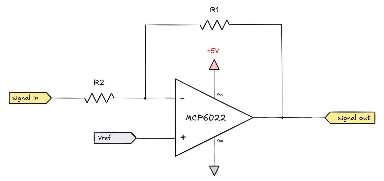
A variation of the basic op-amp topology combines the input voltage and the feedback signal on the same inverting leg:
To analyze the behavior of this circuit, let’s once again assume that R1 and R2 are identical. If the input signal is disconnected, the circuit acts as a voltage follower; given the op-amp’s huge input impedance, the feedback current is negligible, so R1 is not having much of an effect.
If we reconnect the input signal, the situation changes a bit: Vin- is now seeing a 50-50 mix of Vsignal and Vout. If a 100 mV spike arrives from the signal source, it will push the inverting input up by 50 mV. When that happens, the inverting leg is all of sudden more positive, to the amplifier starts reducing its output voltage until it reaches Vin- ≈ Vin+. To compensate for the 50 mV increase on Vin-, Vout would have to drop by 100 mV.
In effect, with R1 = R2, we have an inverting voltage follower; if R1 is increased, the circuit becomes a voltage amplifier with a gain of -R1/R2. As before, because of the presence of a resistor-based divider, the gain is capped at AOL.
The advantage of this circuit topology is that the reference point for amplification is determined by Vref, so we can remove or add DC biases without mucking with the input signal directly. On the flip side, the input impedance of an inverting amplifier is lower due to the feedback resistor connecting Vin- and Vout.
Op-amp frequency considerations
Most general-purpose IC-based amplifiers have a deliberately limited bandwidth: a built-in lowpass filter causes AOL to decrease as the frequency of the input signal goes up, eventually causing the op-amp to stop amplifying once the gain drops below 1x.
Real-world op-amps couldn’t have infinite bandwidth either way, but the reason for a neatly-engineered limit is that the amplifier inevitably exhibits some parasitic, internal capacitances. The capacitances create an apparent sine-wave lag between input and output signals — and thus, a phase shift in the feedback signal normally used to control gain. As the signal frequency increases, this phase delay grows, eventually causing a complete phase reversal — i.e., turning negative feedback positive. If the gain at that frequency isn’t limited, we risk excessive amplification, ringing, or even sustained oscillations once the phase shift approaches one half of the wavelength.
Because of the built-in bandwidth limitations, the datasheet for every op-amp will specify either “unity-gain bandwidth” or “gain-bandwidth product” (GBP). Unity-gain bandwidth is a direct measurement of the frequency at which AOL drops to 1:
The other metric you might encounter — gain-bandwidth product — is extrapolated by observing gain at some lower frequency; for example, if we see 10x at 100 kHz, we can expect 1x at 1 MHz. Both methods typically produce the same result, except if the slope has some kinks in it. This is not common, but can be seen in some high-performance amplifiers where the designer needed to make some trade-offs.
In the case of a well-behaved op-amp and a standard voltage-to-voltage architecture with two resistors, you can take the GBP figure and divide it by the resistor-configured signal gain; the result will be the highest frequency you can pass through without significant attenuation.
As a practical example, let’s say I want to use the TLV4110 op-amp to amplify some audio signal by a factor of 200. The IC has unity-gain bandwidth of 2.7 MHz; at my intended gain, the amplifier should hold up reasonably well to 13.5 kHz (2.7 MHz / 200). While not great, it should be enough to handle medium-definition sound.
Note that this “divide fGBP by signal gain” rule holds true only for simple voltage-to-voltage architectures. For an example of a fairly common op-amp circuit with a very different formula, check out the article on microphone amps.
Another frequency-related characteristic of op-amps is their slew rate — that is, the speed with which they can swing their output from one rail to another. For example, the TLV4110 has a slew rate of 1.5 V/µs; if operated at 10 V, swinging from one rail to another and back would take ~13.3 µs. This understandably limits the ability to amplify large signals at high speed.
As for discrete transistors, the main limiting factor for larger MOSFETs is their gate capacitance: they essentially behave like capacitors that need to be charged or discharged every time you’re changing their gate voltage. For low-power (“signal”) transistors, the capacitance is a couple picofarads; for larger ones, it might be well into the nanofarad range. It follows that power MOSFETs can’t be driven directly by an MCU at higher speeds; problems begin to mount in the kilohertz range. A small transistor- or op-amp preamplifier can help. In any circuit that uses feedback, potential phase lag should be taken into consideration, too.
Amplifier noise considerations
Signal amplification and noise go hand in hand, but a detailed discussion of this topic would make an already-overlong article even harder to digest. In lieu of a deep dive, here are some troubleshooting tips for noisy amplifiers:
Keep any resistance in series with weak signals as low as practical to minimize Johnson–Nyquist noise. It's common for audiophiles to obsess over op-amp noise specs, but the bulk of noise in most high-gain amplifiers comes from resistors.
Use lowpass or bandpass filters to avoid amplifying radio interference or anything else outside the intended frequency band.
Keep all signal wiring short. If you need to run it some distance, use twisted pair or coax.
Use low-ESR decoupling capacitors around high-speed digital circuitry that is a part of the same device — and keep the digital bits at an arm’s length on the PCB. If in doubt, sprinkle 1 µF MLCCs generously across the PCB.
Use ferrite beads on high-speed data busses and on the voltage supply lines ahead of digital circuitry section whenever practical; these can control inrush currents and reduce voltage spikes and EMI.
Make sure you have a good, low-impedance ground path that is uninterrupted and physically close to any high-speed signal lines. This will limit stray electric and magnetic fields. A fully-fledged ground plane or metal shielding can limit some types of issues, too.
Don’t use trashy power supplies. That includes no-name USB wall warts. As a last resort, batteries will always provide cleaner power than a switching power supply.
👉 For a follow-up article dealing with the inner workings of op-amps and current sources, click here. For a practical microphone amplifier circuit, read this article. More on op-amp feedback loops and stability criteria can be found here. Finally, to review the entire series on electronics, check out this page.
I write well-researched, original articles about geek culture, electronic circuit design, algorithms, and more. This day and age, it’s increasingly difficult to reach willing readers via social media and search. If you like the content, please subscribe!











Mate, you made me clever