


Deep dive: the (in)stability of op-amps
A closer look at op-amp feedback loops and the stability criteria for circuits that use them.
This article assumes some familiarity with signal amplification and the knowledge of basic op-amp circuits. If you need a refresher, start here.
In a recent write-up on photodiodes, I mentioned that adding a capacitance in an op-amp’s feedback loop can spell trouble: it might cause ringing, sustained oscillations, or excessive gain.
But… why? It’s easy to offer a hand-wavy explanation of this phenomenon, but the mechanics of amplifier feedback loops are worth a closer look: control feedback is ubiquitous in analog signal processing and can be tricky to get right. Alas, the underlying theory is rather inaccessible to hobbyists; you’re either getting sucked into the discussion of zeroes and poles of complex-number transfer functions, or into obtuse jargon along the lines of this snippet from Analog Devices:
"The amplifier’s stability in a circuit is determined by the noise gain, not the signal gain."
What’s going on here?… What does noise have to do with stability? Not much! If you’re curious, the term has to do with the habit of modeling real-world op-amps as an ideal amplifier with a voltage noise source attached to one of its legs. For some reason, Texas Instruments insists it has to be the non-inverting leg:
“Input voltage noise is always represented by a voltage source in series with the noninverting input.”
So… is “noise gain” just a trade term amplification on that leg? Do op-amps have different gains on each input? How do you set this gain, or where do you find it in the spec?…
All these abstractions make sense in the context of mathematical models, but they don’t build intuition about the real world. In today’s article, let’s talk about feedback loops in a more accessible way. We’ll get to the same results, but hopefully in a less confusing way.
Back to the basics: the open-loop amplifier
Before we proceed, let’s revisit the following rudimentary op-amp circuit:

If you’re here, you should already know the basic behavior of an op-amp: it takes the difference between the two input voltages, amplifies that by some very large number (open-loop gain, AOL), and then outputs the amplified difference as another voltage. Strictly speaking, the output is typically referenced to the midpoint between the power supply rails — let’s call it Vmid — so the complete formula is:
This is the only thing the chip does. Despite the confusing terminology we use to describe op-amp circuits, the IC never pays attention to absolute input voltages, and it can’t be configured to have any other gain.
It is sometimes asserted that an “ideal” op-amp has AOL= ∞. You can find this in Texas Instruments manuals and in some otherwise good books. Pay no mind: this breaks the underlying math. Op-amps, ideal or not, behave correctly only if the gain is finite. You can solve the equations if you assume that AOL is merely approaching infinity, but that’s a different story.
It is true that AOL is normally huge — 100,000 or more — so there’s just a microvolt-range linear region around Vin+ ≈ Vin-. Small variations in this linear region produce a full range of output voltages, but this is nearly impossible to dial in by hand. Any input difference larger than that is bound to send the output all the way toward one of the supply rails. The basic behavior of the circuit pictured above, when supplied with a sine-wave signal, is as follows:

In effect, the op-amp is a voltage comparator: the circuit outputs 0 V when Vin+ drops below Vin- (fixed at 2.5 V), or swings to 5 V otherwise.
For completeness, we should note an important caveat: the capacitances, inductances, and resistances inside any real-world op-amp limit the chip’s response speed. To make the device behave predictably, the designers usually incorporate lowpass filtering that causes AOL to gracefully roll off past a certain point, halving with every doubling of the frequency of an input sine wave. It eventually reaches 1x (unity gain) — and past that point, you’re stuck with an attenuator instead of an amplifier:

The voltage follower
In practice, op-amps are typically employed with some form of a negative feedback loop. The simplest example — a voltage follower with an apparent 1x (unity) gain — is shown below:

At a glance, the circuit seems trivial. The output voltage is looped back onto the inverting input, so if Vin+ > Vout, the differential signal is positive and the output starts creeping up; conversely if Vin+ < Vout, the voltage starts moving down. The process stops once the circuit reaches an equilibrium between all three voltages — essentially forcing Vout to march in the lockstep with the input signal on the Vin+ leg:

Except, this explanation is not quite right. We often take the mental shortcut of assuming that the circuit’s equilibrium is reached at Vin+ = Vin- = Vout — but that’s not actually possible. Remember that at its core, the op-amp is doing the following math:
If the differential voltage is zero, then Vout is constant, no matter the value of AOL. But if Vout (and by extension, Vin-) are stuck in place, then not only is the circuit not doing anything useful, but the differential voltage couldn’t actually be zero. Oops!
What happens in reality that a steady state is reached with Vin- and Vout at a slight offset from the Vin+ input signal. This “error”, when multiplied by AOL, is just enough to produce the correct output voltage. The presence of a negative feedback loop means that any deviations from the stable equilibrium are swiftly countered.
We can figure out the exact magnitude of the offset if we take the op-amp equation and just substitute Vin- with Vout. The substitution just gets rid of an extra variable — and is fair game because in the follower circuit, the two pins are tied together:
The analysis partly vindicates the mental shortcut we have talked about before: when AOL is very high, it follows that 1 / (1 + AOL) ≈ 0 and AOL / (1 + AOL) ≈ 1, so the last expression is kinda-sorta equivalent to:
That said, although the scale of the error nudges is often negligible, ignoring the phenomenon makes the behavior of op-amps difficult to grasp: after all, the nudges are the only thing that is getting amplified! Further, if we actually assume that AOL= ∞, we end up with indeterminate forms in the voltage follower formula, and it all stops making sense.
As noted earlier, saying that AOL merely approaches infinity is OK, but it yields a model that’s needlessly imprecise. As the input signal frequency increases, the internal gain of real-world op-amps drops, so Vout must drift farther away from the target for the sufficient differential voltage to appear across the input pins. In other words, at high frequencies, the output voltage error caused by feedback can get quite high and often needs to be accounted for.
The non-inverting voltage amplifier
Next, let’s look at the usual way of adding gain to a voltage follower:

The operating principle of this circuit is simple: the resistors reduce the voltage on Vin- by a factor of two — so for the input signals to get in the same vicinity, the output voltage has to swing to Vin+ * 2.
The gain configured by the resistors cuts into the op-amp’s AOL, but not for the reason we usually assume. All we’re doing is using some external circuitry to prompt the op-amp to output a different voltage; what does it matter if we’re asking for Vin+ multiplied by 0.5, 7, or -2? The AOL value is a constraint on differential gain, not on the relation between Vout and Vin+. Signal gain is free! The chip don’t care!
The problem lies elsewhere: the resistors attenuate the nudges that piggyback on top of the output signal. It used to be that Vin+ and Vout needed to differ only by some small amount to encode a full range of input voltages; let’s call that difference Vdiff. Now, because of the added attenuation, we need Vdiff * 2 to achieve the same result. This is akin to replacing the op-amp with a chip that has half the AOL we started with. If we push the configured amplification far enough, the effective AOL drops below 1, and at that point, Vdiff would need to swing past the supply rails to produce a full range of output voltages. In most circuits, that’s not happening.
The fine point about attenuated differential signals might seem like an academic distinction, but there are less common op-amp circuits where signal amplification is done differently does not come at the expense of AOL.
Understanding loop gain
As should be clear by now, the feedback loop doesn’t actually change the op-amp’s gain. All we’re doing is offsetting Vin+ from Vin- in a specific way. In the closed-loop configuration, the chip’s internal amplification remains very high — and for the sake of signal accuracy, we want it to stay that way!
In a way, the feedback nudges can be thought of having their own gain, separate from any signal amplification configured by the designer of the circuit. For example, in the case of a voltage follower, the configured signal gain is 1x, while the amplification of the feedback “error” is in the vicinity of AOL. Conversely, if we max out signal gain by adding resistors in the feedback loop, Vdiff needs to swing quite a bit and the apparent feedback loop gain is low.
For the standard voltage amplifier topology, the magnitude of loop gain is proportional to the vertical distance between the op-amp’s intrinsic amplification curve and the circuit’s configured voltage gain (in our example, 1x):

At this point, we have a preliminary explanation of one of the more counterintuitive properties of op-amps: that instability and some types of noise problems can get worse at lower signal amplification rates. The higher the gain in the feedback loop, the more faint are the differential control voltages, and the more pronounced are the consequences of any small signal errors introduced along that path.
The tape-delay op-amp circuit
This brings us to the following unorthodox design:

It’s a voltage follower — except for a contraption that records output voltages and plays them back some time later on the Vin- side, delaying the feedback signal by a preset amount. A temporal defect in the loop!
To explore this circuit, I built a toy discrete-time model with a limited bandwidth and a feedback loop that lags by five “ticks”. I then supplied a single input pulse on Vin+ and let the simulation run:
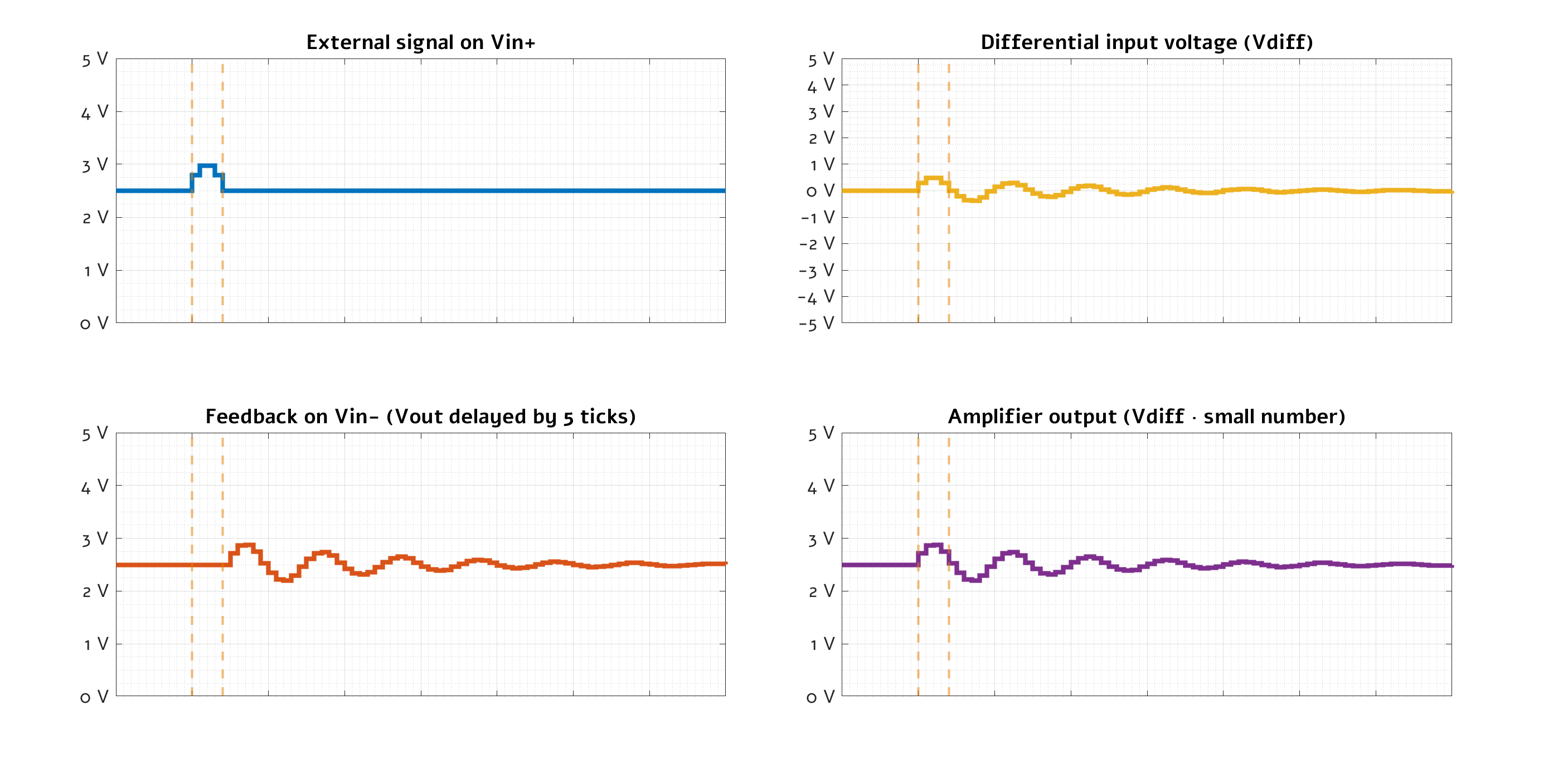
For the first five ticks, Vin+ (blue) is seeing a positive pulse while Vin- (red) is staying put due to the delay. As a consequence, Vout shoots up — although because of the baked-in bandwidth limit, it does not immediately jump all the way to +5 V.
After five ticks, Vin+ goes back to the mid-point and stays there for the rest of the simulation — but all of sudden, the delayed echo of the last pulse arrives on Vin-. It pulls the differential voltage negative, thus producing an inverted echo on the output. This back-and-forth process continues for a while, with gradually decaying amplitude.
The most important observation is that past the initial stimulus, the entire action is contained to the feedback loop. There is no movement on the signal input (Vin+), so the configured signal gain plays no role. The only reason the oscillations decay over time is that at the offending “echo” frequency, the gain of the feedback loop itself happened to be a tad below one.
If we increase loop gain a tiny bit, we get this result:
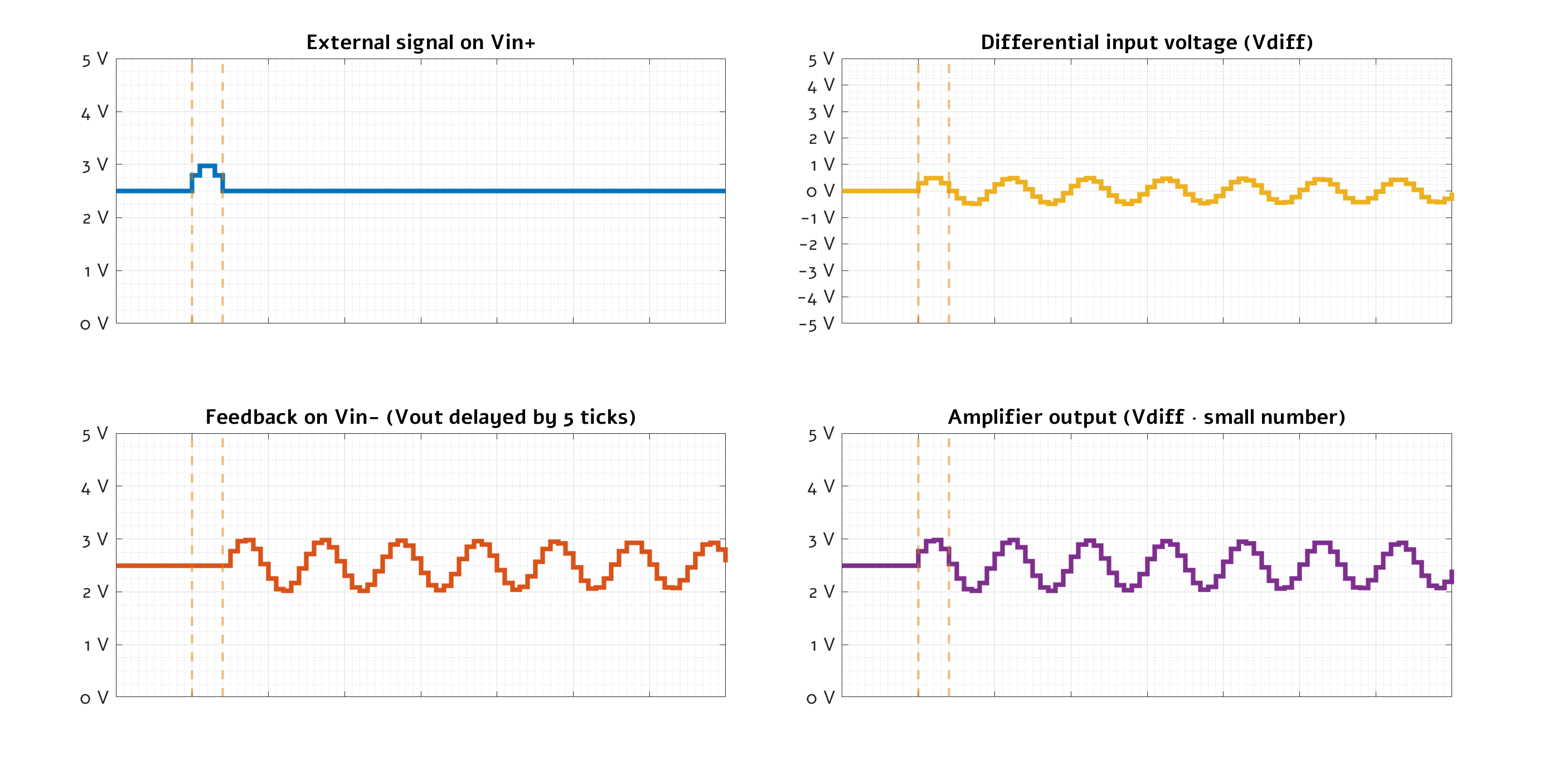
There are two conditions that must be met for sustained oscillation:
There must be a feedback delay of about one-half of a wavelength (180°) at some sine-wave frequency.
The feedback loop gain at that frequency must be at least one.
The first requirement means that higher frequencies are of more concern, because it’s easier to accidentally introduce comparatively large delays when the wavelength you’re working with is short. The second requirement means that we generally only have to worry about the frequencies below the IC’s internal unity-gain point.
But what kind of a weird contraption is that?!
Right. Tape-delay mechanisms are not commonly employed in op-amp circuits. Non-negligible transmission delays can sometimes crop up in electronic designs, but feedback loops are usually pretty compact on any sensibly-designed PCB. Unless you’re working with ultra-high frequencies or very long wires, signal propagation times are a relatively remote concern.
Yet, there is another, more ubiquitous form of a “delay” mechanism: the capacitor. To be clear, a capacitor is not really a time delay device: it can’t store and replay past waveforms. Instead, it’s an integrator — that is, its terminal voltage is a function of the charging currents that flowed through it before. It might sound math-y, but it’s akin to how a bucket in your backyard “integrates” rainfall over time, “outputting” the result as a water level you can observe.
Integration distorts most waveforms — but in the special case of a sine, it just produces a phase shift:

The phase shift pictured above is between the charging current and the terminal voltage. Current per se is not commonly used to convey information in electronic circuits, but if a capacitor is charged and discharged through a resistor, then from Ohm’s law, the admitted current is proportional to the applied voltage. In effect, in such a layout, there is some degree of voltage shift between the driving sine and the output sine. The shift varies from 0° to 90°, depending on R and C values and signal frequency; a detailed discussion of this phenomenon can be found in an earlier article.
Such a phase shift can be observed when shunt capacitances are added to op-amp feedback loops even without any discrete resistors. That’s because the amplifier’s output transistors have some non-zero impedance (ZO or RO in the spec). The number often hovers around 20 to 100 Ω; this acts like a hidden series resistor in the output path.
On the surface of it, even the worst-case RC shift (~90°) is nowhere near the ~180° offset needed for sustained oscillation — but op-amps have some internal phase shifts too. The devices are usually designed so that their bandwidth rolls off just ahead of the danger zone, leaving just a bit of phase margin for external components. With some ICs, even as little as an extra -45° can be enough to put you in the red.
When that happens, short of reducing the capacitance, some of the hacks may involve reducing the bandwidth of the feedback loop; bumping up signal gain; or switching to a more capable amplifier that has more of a phase margin at the frequencies of concern.
👉 For a thematic catalog of articles on electronics and other topics, click here.
I write well-researched, original articles about geek culture, electronic circuit design, and more. If you like the content, please subscribe. It’s increasingly difficult to stay in touch with readers via social media; my typical post on X is shown to less than 5% of my followers and gets a ~0.2% clickthrough rate.