


Shining light on photodiodes
A quick intro and an application circuit for a versatile but oft-misused light-sensing component.
Let’s say you want to build a circuit that measures ambient illumination or receives data via an optical link. Today, if you start researching the topic, there’s a good chance you end up on a page filled with inane, AI-generated slop:
“Some phototransistors, especially the older models, are not capable of handling voltages higher than 1,000 Volts. “
“The last disadvantage of phototransistors is that the electrons in them do not move as freely as in other transistors. […] Because of this limitation, phototransistors are typically more expensive than regular transistors.”
Hit “back”, select another result, and experience a serious case of deja vu:
“Silicon-based phototransistors cannot handle voltages exceeding 1,000 Volts.”
“Furthermore, they do not allow electrons to move as freely as other devices like electron tubes.”
Hold up, let’s try another site:
“While phototransistors can be advantageous, they also have several disadvantages. Phototransistors made of silicon cannot handle voltages over 1,000 Volts. They do not allow electrons to move as freely as other devices, such as electron tubes, do.”
Even on websites that are written in good faith, some pain awaits. For example, almost every source insists on making a pointless distinction between “photovoltaic” and “photoconductive” operating modes of a semiconductor junction — never really explaining the difference, and then doubling down with nonsensical V-I plots that don’t have any conceivable real-world use.
In today’s episode, let’s do better. We’re going to focus on photodiodes, as they are the most versatile yet tricky of the general-purpose light-sensing elements.
Back to the basics: the p-n junction
To explain photodiodes, we need to start with a quick recap of the physics of conduction.
In non-conductive materials, the outer electrons are bound tightly to individual molecules; a considerable amount of energy is needed to make them hop from one molecule to another. In metals, the most energetic electrons are not tied to any specific atom. They occupy the so-called conduction band and can move back and forth in response to external electric fields.
Semiconductors are an in-between case: the energy difference between the energy bands is so minor that some valence electrons are regularly knocked into the conduction band due to room-temperature thermal effects. That said, in pure (“intrinsic”) semiconductors, these charge carriers are short-lived and not particularly plentiful, so the resulting conductivity is poor.
This changes with the addition of carefully-selected impurities (dopants). In an n-type semiconductor, the dopant increases the number of long-lived conduction-band electrons. In a p-type semiconductor, a different additive creates valence band vacancies (“holes”) that allow lower-energy electrons to shuffle around in response to external fields; this can also be thought as the holes “drifting” the opposite way. Both types of doped materials conduct electricity surprisingly well.
A standard semiconductor diode is formed by bringing together a p-type material and an n-type material. In a very narrow boundary region, n-side electrons diffuse into the p-type semiconductor and promptly fall into valence-band holes, emitting a photon on the way:

This process results in an unbalanced electric field that’s wholly contained to the depletion region. The field prevents majority charge carriers from venturing across, rendering the diode nominally non-conductive.
Plucking the electrons from the right (cathode) and depositing them on the left (anode) doesn’t accomplish much. It adds an electric field identical to that present in the depletion region, making it harder for majority charge carriers to skate across. When connected this way (“reverse-biased”, cathode more positive than anode), the diode will not conduct — at least not until some form of a breakdown occurs.
Going the other way round is another story. If the anode is made more positive, it offsets the junction’s internal field — eventually reducing it enough to let charge carriers cross the divide. For a typical silicon diode, this “forward” threshold is about 0.6 V.
The miracle of photocurrent
If electrons falling into a lower energy state emit photons, it’s probably unsurprising that the opposite can happen too: shining light on a semiconductor can knock some electrons into the conduction band. And if this excitation happens in the p-n junction’s depletion region, the existing internal electric field immediately accelerates the electron and tosses it over to the n-type (cathode) side. Meanwhile, the positively-charge hole is jettisoned to the other side.
In an open-circuit scenario — that is, if the diode’s terminals are not connected to anything — exposing the junction to light causes a small voltage to gradually build up within the component. The resulting field inevitably shrinks the depletion region, so the effect is non-linear and self-limiting — but it’s quite easy to observe with a multimeter and a source of light.
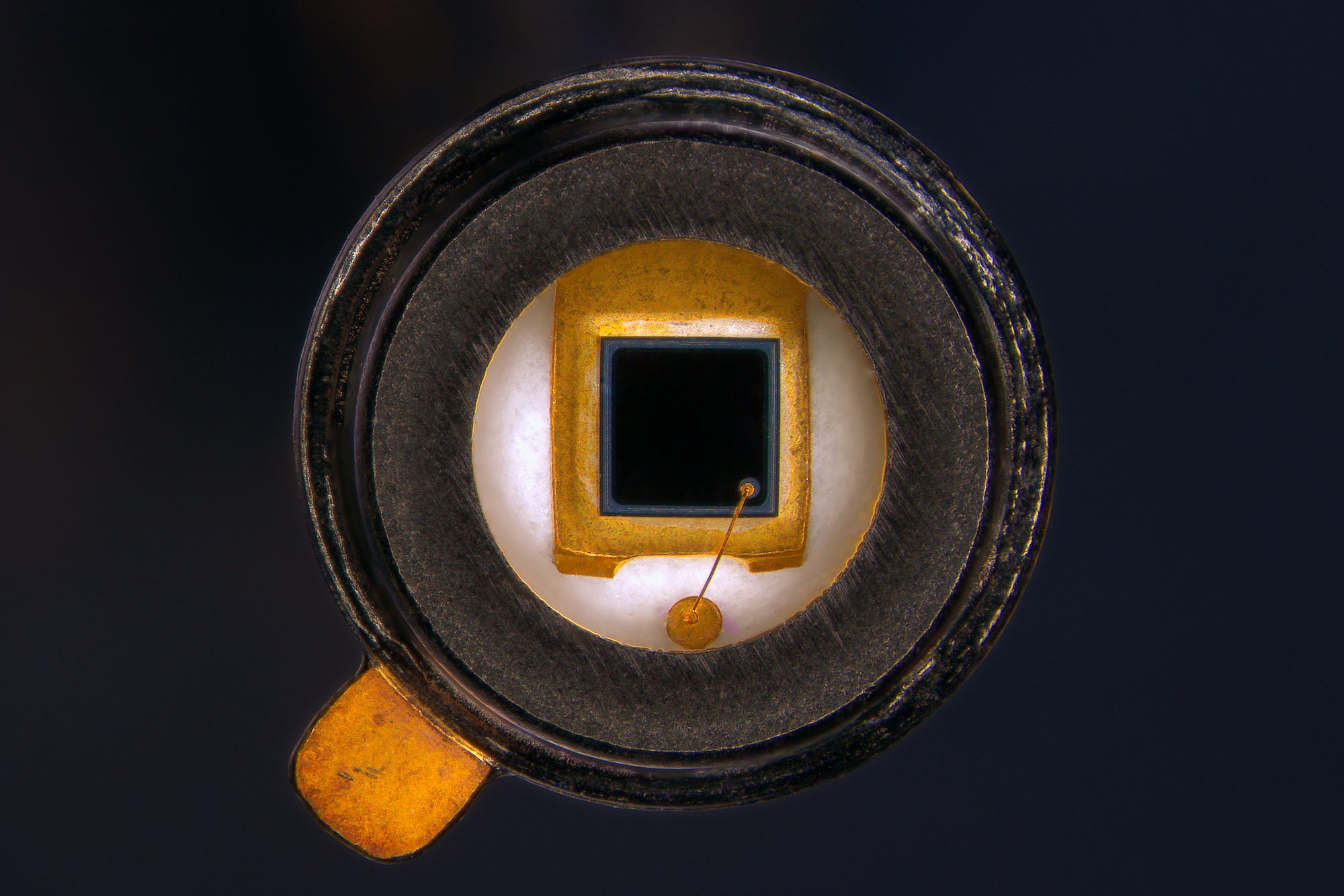
To illustrate, I placed a Marktech MT03-023 photodiode directly in front of a small, generic white LED. I connected the photodiode to a precise benchtop multimeter, and then used a signal generator to drive the LED with a smoothed 10 kHz square wave:

Alas, not only are the readings nonlinear, but at lower light levels, they simply cannot be trusted. In complete darkness, the photodiode behaves essentially like an open circuit — so stray voltages can build up due to RF interference, static electricity, and so forth.
To avoid these problems, the terminals of a photodiode should be shunted via some comparatively small impedance instead. In this mode, the device is free to keep moving charge carriers at the exact rate they’re created. If we plot shunt current as a function of light intensity, we get a supremely linear plot in conditions ranging from sunlight to candlelight:

It’s important to note that the photocurrent generated by the diode has a polarity opposite to the normal induced current through a forward-biased diode: electrons flow out of the cathode.
Building a photodiode amplifier
The main issue with photodiodes is that the currents they generate are fairly miniscule — at least until we scale the devices up to the size of solar panels (hey, it’s the same operating principle!).
To get the most out of a reasonably-sized photodiode, we need a linear, low-noise current-to-voltage (“transimpedance”) amplifier. A single-supply circuit employing a modern rail-to-rail (RRIO) op-amp, such as OPA2323, can be constructed the following way:

First, note that the photodiode’s anode is connected to the ground. There are no negative supplies in this circuit, so we know the diode can never be forward-biased, and never conducts in the conventional direction. It works solely as a photocurrent generator.
In a darkened room, the photodiode shouldn’t be doing anything of note; in a steady state, the series capacitor is also of no consequence. In effect, for the initial analysis, we can ignore the grayed-out parts:

Op-amp afficionados should immediately recognize the remaining bits as a voltage follower (if you need a refresher on op-amps, click here). In essence, with the diode out of the picture, the amplifier is “following” (i.e., outputting) a fixed 0 V signal that’s present on its non-inverting leg.
The situation changes in the presence of a photocurrent. The diode starts moving electrons from the GND side toward the inverting input of the op-amp, making Vin- slightly more negative. Because Vin- is now lower than Vin+, the output voltage starts rising. And because Vout > Vin-, some current starts flowing via the feedback resistor (Rf), pulling Vin- back up.
The equilibrium is reached when the Rf current matches the photocurrent, essentially canceling out the influence of the photodiode. Per Ohm’s law, the output voltage swing needed to produce that feedback current is directly proportional to the value of Rf — e.g., a 100 kΩ resistor turns a 10 µA photocurrent to an output swing of 1 V.
Additional circuit notes
Conventional (non-RRIO) operational amplifiers may not work if their inputs or outputs are too close to the negative supply rail. Further, even in modern rail-to-rail op-amps, the output stage usually can’t reach true 0 V; for example, OPA2323 bottoms out at 30 mV. In the absence of sufficient photocurrent, this makes Vin- slightly positive, diminishing the response to low illumination levels — and hurting response speed by placing the op-amp outside its linear operation regime.
In both cases, the problem can be solved by creating a small offset voltage — perhaps 0.5 V — and applying it to the non-inverting leg:

As should be evident from the earlier voltage follower analysis, the 0.5 V offset present on Vin+ will carry to the output, thus moving all three voltages some distance from the negative supply rail. Some dynamic range will be lost — but with a simple single-stage architecture, them’s the breaks.
As discussed in the article on microphone amplifiers, the bandwidth of transimpedance amplifiers is derated differently than in the case of a more common voltage-to-voltage circuit. The amplification still tapers off at higher frequencies, but gain at lower frequencies comes nearly free, until subverted by parasitic capacitances. The maximum cutoff point is given by the following formula:
In this equation, fGBP is the op-amp’s gain bandwidth product (taken from the spec); Rf is the value of the feedback resistor that sets the amplification ratio; and Cin is the input capacitance (including op-amp parasitics). In our case, with a 20 MHz amplifier (OPA2323), a 50 kΩ resistor, and a small photodiode that exhibits junction capacitance around 20 pF, the resulting signal bandwidth should be a tad under 2 MHz.
As for the non-trivial capacitance of the diode: it behaves that way because it consists of two conductive regions separated by a very thin insulator layer. To offset the undesirable effects of this capacitance, a small lowpass capacitor — Cf in the schematics above — is meant to lower gain at high frequencies by shunting Rf just as Cin is starting to pull the circuit the other way.
There is a fair amount of esoteric theory and lingo that underpins the modeling of op-amp feedback loops, but for the purpose of this article, we can just select the maximum Cf capacitance that still works for the highest signal frequency you expect to be dealing with (fpass). The formula is:
It is also possible to calculate the minimum Cf value that keeps gain peaking within certain limits. The most common formula for a reasonably flat frequency response (Q = 1) is:
For a maximally-flat (Butterworth) response, 2π must be replaced with 4π.
In this particular case, in a typical photodiode circuit with a fast op-amp and an input capacitance measured in tens of picofarads, several pF in the feedback loop are enough to make the circuit behave. The lowpass effect of higher capacitances just helps reduce noise.
Another way to lower the diode’s capacitance without sacrificing bandwidth is to connect the anode to a lower voltage. This widens the depletion layer; reverse-biasing with -5 V to -10 V is well-tolerated by most diodes. The modification will cause some constant quiescent (dark) current through the junction, but — within the limits of reason — it will not hurt linearity.
(Another clever bandwidth hack is to use another amp to make the diode capacitance disappear.)
Should I even be using a photodiode?
Photodiodes are the best option if you need to make fast, accurate, and linear readings with a wide dynamic range. The diodes’ spectral characteristics are not linear — that is, they are more sensitive to certain wavelengths — but this can be addressed with color filters or buying a diode tuned for a specific use.
A phototransistor works quite similarly to a photodiode: most commonly, it’s a see-through bipolar NPN, driven by an internal photocurrent in lieu of having a standard base terminal. This architecture has a built-in current gain, so compared to a photodiode, you save on an amplifier. That said, this crude form of amplification is not particularly linear, the dynamic range is limited, and the response time is considerably slower. Because of these limitations, phototransistors are most commonly used for “binary” sensing in electromechanical devices — photointerrupters, barcode readers, and so forth.
Finally, photoresistors (or light-dependent resistors, LDRs) are made from monolithic, junction-free semiconductor materials, most commonly cadmium sulfide. Their resistance decreases when exposed to light due to the excitation of electrons. They’re the OGs of light measurement; they’re hard to kill and easy to use. That said, LDRs are not especially linear and tend to be excruciatingly slow, with response times measured in hundreds of milliseconds. They’re OK for sunlight sensors and other simple devices, but they’re not as popular as they used to be.
👉 Continue reading about photodiodes: see this article for a circuit that eliminates the sensor’s capacitance, click here for a semi-practical photodiode project, or read more about photodiode response times.
I write well-researched, original articles about geek culture, electronic circuit design, and more. If you like the content, please subscribe. It’s increasingly difficult to stay in touch with readers via social media; my typical post on X is shown to less than 5% of my followers and gets a ~0.2% clickthrough rate.
Something I was planning to mention, but that didn't make the cut: regular LEDs work as (poor) photodiodes too, with a LED-color-specific spectral response. Experimental results can be found here:
https://learnmaketeachshare.org/sensors%20and%20circuits/2018/10/30/using-leds-to-measure-narrow-spectral-bands.html
As for photodiode response times: they're usually given in the spec, but values between 1 and 100 nanoseconds are common for small devices. Some tiny BGA units will have response times as low as 100 ps; while large, specialty sensors may be as slow as a microsecond or so.
Great articles as always. I found this other nice article explaining how to measure small currents with just the ADC and microcontroller pin capacitance and thought you might enjoy it. https://community.silabs.com/s/article/using-adc-to-measure-a-current-source-with-no-external-components?language=en_US
In my own testing it seems to still be very sensitive to noise, but I'm also using 1 inch long through hole LEDs flapping in the breeze. I was able to mostly work around it by using another LED painted black and subtracting the values, but I'm trying to anticipate what will happen when they become tiny SMD components on a PCB and if the floating input will be a problem still. My application requires ~10000x dynamic range, which makes things interesting too and is perfect for the ADC method above.