Building a phosphorescence detector
There's very little written about natural phosphorescence. Let's design a device that can spot it in the wild.
Some time ago, my eldest son decided to make glow-in-the-dark pigments by doping strontium aluminate with rare earth elements. After a bit of trial and error, he succeeded — and the relative simplicity of the process made me wonder if there are any naturally-phosphorescent materials in our homes.
Of course, we’re not surrounded by items that exhibit strong and long-lived phosphorescence. Still, perhaps the effect is too faint or too brief to see with a naked eye? The internet offered no good answers, so I decided to investigate on my own.
Note: I reworked this article after publication. The revised text talks about some of the original project challenges, and then presents an improved version of the design.
The detection chamber
The basic idea was simple: place samples in a lightproof container, shine a UV light on them, and then measure the afterglow with a photodiode. I picked a UV source because both fluorescence and phosphorescence usually involve secondary emissions at lower energy levels; ultraviolet has higher photon energies than the visible spectrum or IR.
The first gotcha with the design is the inherent trade-off between sensitivity and response speed. A photodiode with a large active area is more sensitive, but has a high junction capacitance, notionally making it harder to capture short-lived events. In contrast, a small photodiode is fast, but needs more amplification; faint readings are more easily drowned out by noise.
Based on a gut feeling, I decided to go for speed: I figured I want to be able to measure down to a microsecond, so I bought a Marktech MT03-023 photodiode with a 1.2 mm² die and a 20 pF junction capacitance. I fashioned a test chamber out of a round tin can, drilling holes in the lid to accommodate UV LEDs and the sensors. My initial prototype used a single photodiode and four 385 nm LEDs (VAOL-5GUV8T4), but I wasn’t happy with the sensitivity, so I upgraded to ten UV emitters and two photodiodes in parallel:
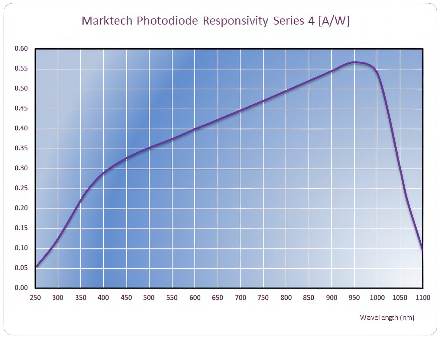
Speed aside, I picked these photodiodes because of their good sensitivity on the blue-green end of the visible spectrum — about four times higher than for a run-of-the-mill silicon diode:
The power architecture
I originally planned for a single-supply circuit. Before long, I was juggling four different power domains:
In this design, a cheap 5 V wall wart provides power for the LEDs and for the bulk of the digital circuitry (Vdd_5.0). I wanted to shield amplifiers from digital switching transients, so I also created a second 5 V domain — Vclean_5.0 — and separated it from the icky digital bits with a ferrite bead (B-06-R-25) and some capacitors.
After constructing the first prototype of the device, I noticed that the amplified sensor readings took more than 200 microseconds to settle on a stable output value. I spent a fair amount of time debugging the issue; I eventually noticed that the current needed by the UV lights caused the PSU voltage to sag by about 40 mV. The recovery was sluggish, too:
Op-amps and digital chips are relatively immune to slow fluctuations of the supply voltage, but I was also using this rail for biasing and to provide a reference for the analog-to-digital converter (ADC). This caused the ripple to be amplified alongside with the signal I cared about.
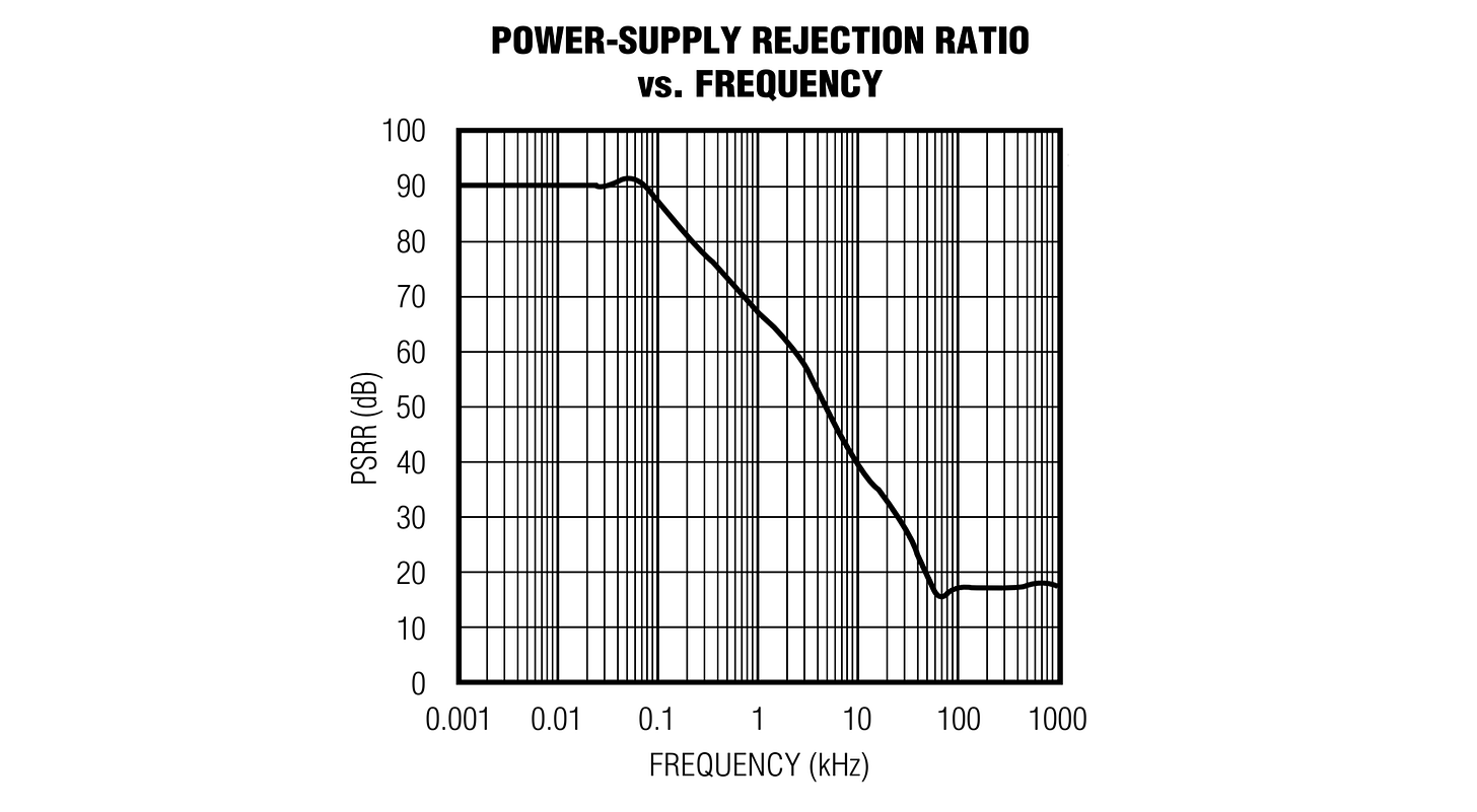
To fix the problem, I grabbed a device known as a “series bandgap reference” (MCP1501-45E) — an integrated circuit that exploits the inherent electric field of a semiconductor junction to output a stable, precisely-trimmed voltage. Or at least, that’s the theory; buried in the spec for such chips, you usually find a curve that looks the following way:
A power-supply rejection ratio (PSRR) of 90 dB means that any supply-side glitches are attenuated by a factor of ~30,000 (i.e., 40 mV → 1.3 µV); at 15 dB, the factor drops to just ~5x (40 mV → 8 mV). In other words, such ICs are great at suppressing supply low sine-wave frequencies, but might start sucking by the time you approach 10 kHz.
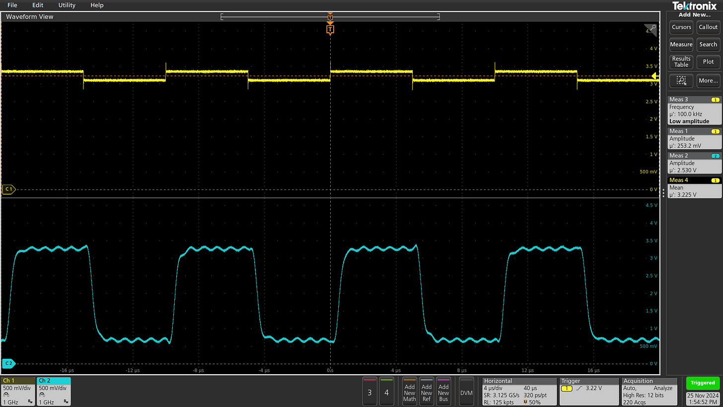
To illustrate this effect in real life, let’s have a look at the behavior of MCP1501 in the presence of a bunch of (synthetic) load-switching ripples on the IC’s supply pin:
After every edge, the regulator needs about 50 µs to catch up. The simplest workaround is a beefy RC lowpass filter on the input or output side. I’m using 220 Ω + 10 µF on the output; this produces 98-fold ripple attenuation at 5 kHz without seriously impeding the sub-1 mA load on this rail.
The final voltage domain in the circuit is Vadc_1.8. The story behind it is simple: I bought an ADC that needs 1.8 V for the analog parts. There are single-supply ADCs with comparable specs, but they cost more. A standard linear regulator (MCP1700-1802) saves the day. The ADC has a fairly high PSRR, so the stability of this supply is less critical, but a bit of filtering is incorporated just in case.
The amplifier
As per the primer on signal amplification, the advertised bandwidth of an operational amplifier must be derated proportionally to the desired signal gain. In other words, to rapidly measure the miniscule currents produced by a photodiode, we need to start with a pretty fast chip.
I scoured my parts bin and picked TLV354x — a neat rail-to-rail op-amp with an advertised bandwidth (fGBP) of 100 MHz:
The architecture of this circuit follows the blueprint outlined in a recent article on photodiodes. The right-hand part is a transimpedance amp (TIA) that produces an output voltage proportional to diode photocurrent times 220,000 (4.5 µA → 1 V). There is also a small offset (160 mV) added on the Vin+ leg; this is to keep the TIA within its specified output range. The voltage follower section (left) is a “bootstrap” that removes photodiode capacitance (40 pF) and replaces it with that of an op-amp input (3-4 pF); it’s a performance-enhancing trick previously discussed here.
In this configuration, the maximum attainable TIA bandwidth hovers around 4 MHz:
That said, to avoid amplifying excess RFI and resistor noise, it’s further limited to around 1 MHz by the feedback capacitance. The two 1 pF caps in series are equivalent to a single 500 fF capacitor; it’s done this way because I don’t have any femtofarad-range caps at hand. Another 100-200 fF is probably added by the feedback resistor. The math is the standard RC filter formula:
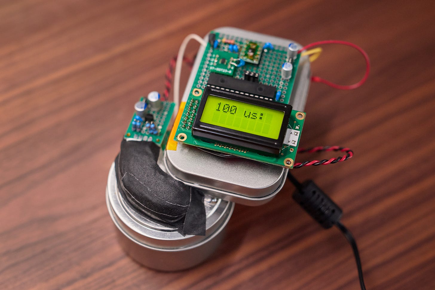
To keep radio interference in check, the entire amplification stage is housed in another Altoids-style can, soldered on top of the test chamber and bonded to circuit ground. When designing the initial prototype, I noticed that in the absence of RF shielding, the circuit would pick up electrical noise from household lighting — about 200 mVp-p:
Some readers might be wondering why I’m not pushing amplification any further; feedback resistances all the way to 800 kΩ still satisfy the TIA bandwidth formula. The gotcha is Ohm’s law: I = V/R. The higher the resistance, the less current can be pushed through the feedback path before Vout hits the supply rail. If the op-amp can no longer match the photocurrent, input voltages get out of whack and the entire TIA abstraction falls apart. We need Rf small enough so that under normal operating conditions, Vout stays in the linear regime.
The photodiode surprise
The circuit worked, but there was a gotcha: the output waveform was taking longer to settle than standard op-amp math would dictate. My expectation was a settling time around 1 µs. In practice, the signal needed nearly 20 µs to shed the last 10 mV of the falling edge:
This sent me on a multi-day wild goose chase that’s described in this companion article. Briefly: the response of a photodiode is actually a sum of two currents: a nearly-instantaneous drift current involving photon-created electron-hole pairs in the p-n junction’s depletion region; and a weaker, slow diffusion current due to minority charge carriers that are into existence outside the active zone, and that randomly stumble into the depletion region’s electric field some time after the light is turned off.
There is no real solution to this problem; reverse-biasing the diode decreases the magnitude of the effect, but doesn’t make it go away. The only practical answer is software compensation. The shape of the curve depends on the “LED on” time and on how much light was hitting the photodiode, so to calculate the offset, we need to keep track of both.
The last (analog) mile
My original design used a two-stage op-amp architecture, but that was before I knew about the need to compensate for diffusion currents. Now that I needed to measure the peak photocurrent — which depended on the reflectivity of the sample under test — I couldn’t just add a second amplifier that teases out low-light readings, but clips all the “LED on” data at 5 V.
I briefly considered a dual-ADC approach, with one converter plugged in between the amplifier stages to take the “on” readings, and then a second one to measure the afterglow. But another way to get the same information is to forgo the second stage altogether, and simply digitize the TIA output with better resolution.
To that effect, I traded the original 14-bit ADC (MCP33151-10) for a more expensive 16-bit model (MCP33131-10). I then implemented repeated sampling and averaging to add another two bits.
Normal average (arithmetic mean) is easily skewed by individual outlier readings caused by strong pulse-like RFI noise. To avoid this, the software records a preset number of ADC acquisitions (m), sorts the values, and then picks a band of n elements centered around the midpoint of the buffer. The case of n = 1 is just the median, but n > 1 improves resolution at no cost. I’m using n = m / 10.
To keep things moving, I also used a measurement optimization strategy: I turned the LEDs on for a couple of seconds to fully “charge” the specimen, and then started pulsing them on and off while maintaining an overall high duty cycle. For example, to measure the average glow at 2 µs, the code repeatedly turns the LEDs off for 2 µs, performs an ADC conversion, and then turns them back on for 1 ms. Because the effective duty cycle is 99.8%, there is no risk of the material losing charge.
The MCU side
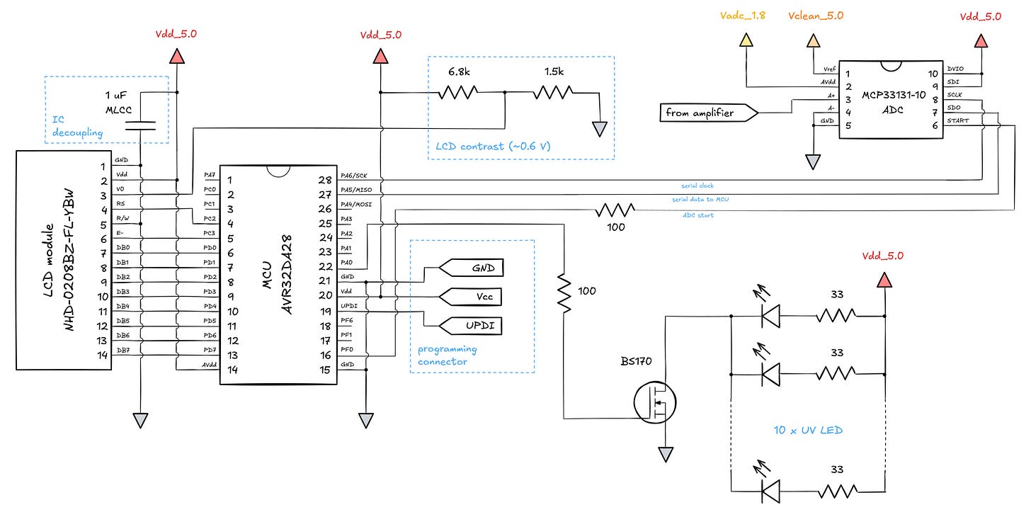
The digital part of the circuit is fairly straightforward. I’m using an AVR Dx series microcontroller running at 24 MHz to talk to the ADC over the serial peripheral interface (SPI). The MCU is also connected to a text-based LCD that follows the common Hitachi HD44780 protocol over an 8-bit parallel bus:
The resistors on two control lines were added to reduce high-frequency transients around the time of the ADC conversion. The remaining digital lines are operated on a schedule that doesn’t jeopardize photodiode readings.
The photodiodes are toggled by a pretty standard, small n-channel MOSFET (BS170). It can be substituted freely, although power MOSFETs with high gate capacitances should be avoided, as they would lower switching speed.
The (mildly disappointing) results so far
My first test involved a plastic glow-in-the-dark trinket dyed with zinc sulfide. The measurements are shown below:
Although the object glows in the dark for a good while, the intensity of the effect already decays exponentially on a sub-millisecond scale.
After this, I scoured the kitchen for test materials. I tested a fair amount of condiments, but I had no meaningful readings on most. One of the finds that exhibited pretty strong phosphorescence was powdered milk:
The plot is quite similar to the earlier one, but the effect is about two orders of magnitude weaker; the glow is actually visible with a naked eye, but only in total darkness and only for about a second after hitting the material with a UV beam.
Another unexpected glow-in-the-dark foodstuff? Gelatin! It initially registered about 30% higher than powdered milk, but decayed more quickly.
Elsewhere in the home, in my kids’ mineral collection, an unassuming chip of natural ruby exhibited surprisingly strong phosphorescence — yielding an ADC reading of about 2,000 at the 100 µs mark, then decaying to almost nothing at 20 ms.
That said, I came across two items that exhibit weak but perceptible phosphorescence, yet don’t register with the circuit: an odd jar of almond butter and a random piece of rock. I’m not quite sure what the issue is; my eldest son’s bet is that there’s just not enough photons hitting the photodiode.
👉 For a thematic catalog of articles on electronics, gear-making, and assorted other topics, click here.
I write well-researched, original articles about geek culture, electronic circuit design, and more. If you like the content, please subscribe. It’s increasingly difficult to stay in touch with readers via social media; my typical post on X is shown to less than 5% of my followers and gets a ~0.2% clickthrough rate.









In the 1980s I worked for marine biologists who used fluorometers to measure chlorophyll in the open ocean at concentrations of micrograms per litre in seawater. The lab instuments used a photomultiplier tube detector -which was impractical to package for conducting chlorophyll profiles of the water column using an instument package the was to measure down to 200 meters or so. So, the instrument we used made by Sea-Tech which used xenon flash excitation and a large photodiode along with optical filters to limit the excitation band to around 425nm and the receiver band to 685nm. The receiver had a sample and hold/peak detector to capture the received 685nm energy flourescing from any chlorophyll bearing biomass in the water.
It worked but it was noisy. It was difficult to eliminate noise emmitted by the flash circuit, and the sample and hold - not to mention the clumpy nature of chlorophyll bearing criters distributed in the water column.
These were hand built, expensive instruments. I made an attempt to build a cheapo instrument that used blue LEDs as emmitters and a red LED as a detector. The red LED was used as a photo generated current source meant to drive a current-to-frequency converter (Op Amp + 7555 timer chip). Frequency variation was to offer some measure of chlorophyll content. The setup would be calibrated against the lab fluorometer. I never got past a protoype. It sort of worked but was probably not sensitive enough.
I'm sure you know this, but peanut butter phosphoresces (relatively) strongly