


Lies, damned lies, and photodiodes
Diffusion and drift currents: depending on what you're trying to do, photodiodes can be really fast or infuriatingly slow.
This article is a part of a series on photodiodes. To start from the beginning, click here.
If you’re tinkering with photodiodes, you might be wondering just how fast these devices are. The specs always make it seem simple: they cite a “response time” figure, and for a general-purpose sensor, it’s probably between 10 and 150 ns. What’s the testing methodology? Oh, don’t you worry your pretty little head! Every manufacturer is doing it in a different way.
Dig a bit deeper and most of the accessible literature will point you to the capacitance of the p-n junction inside the device as the main bottleneck. This is a bit of a red herring: the capacitance matters, but it can be drastically reduced. A simple hack is to apply a reverse bias to the junction; the bias widens the depletion region, effectively pulling the “plates” of the imaginary capacitor apart. A better if less-known solution is to use a clever “bootstrap” topology that keeps the diode’s terminals at the same potential, rendering the capacitance irrelevant.
But then, if you’re attempting to build a precision measurement device, there’s another issue they don’t tell you about: there are two types of photodiode current, and they behave in different ways. It bit me hard when working on a revised version of my phosphorescence detector, and I think it’s interesting enough to deserve its own post.
The mysteriously subpar amplifier
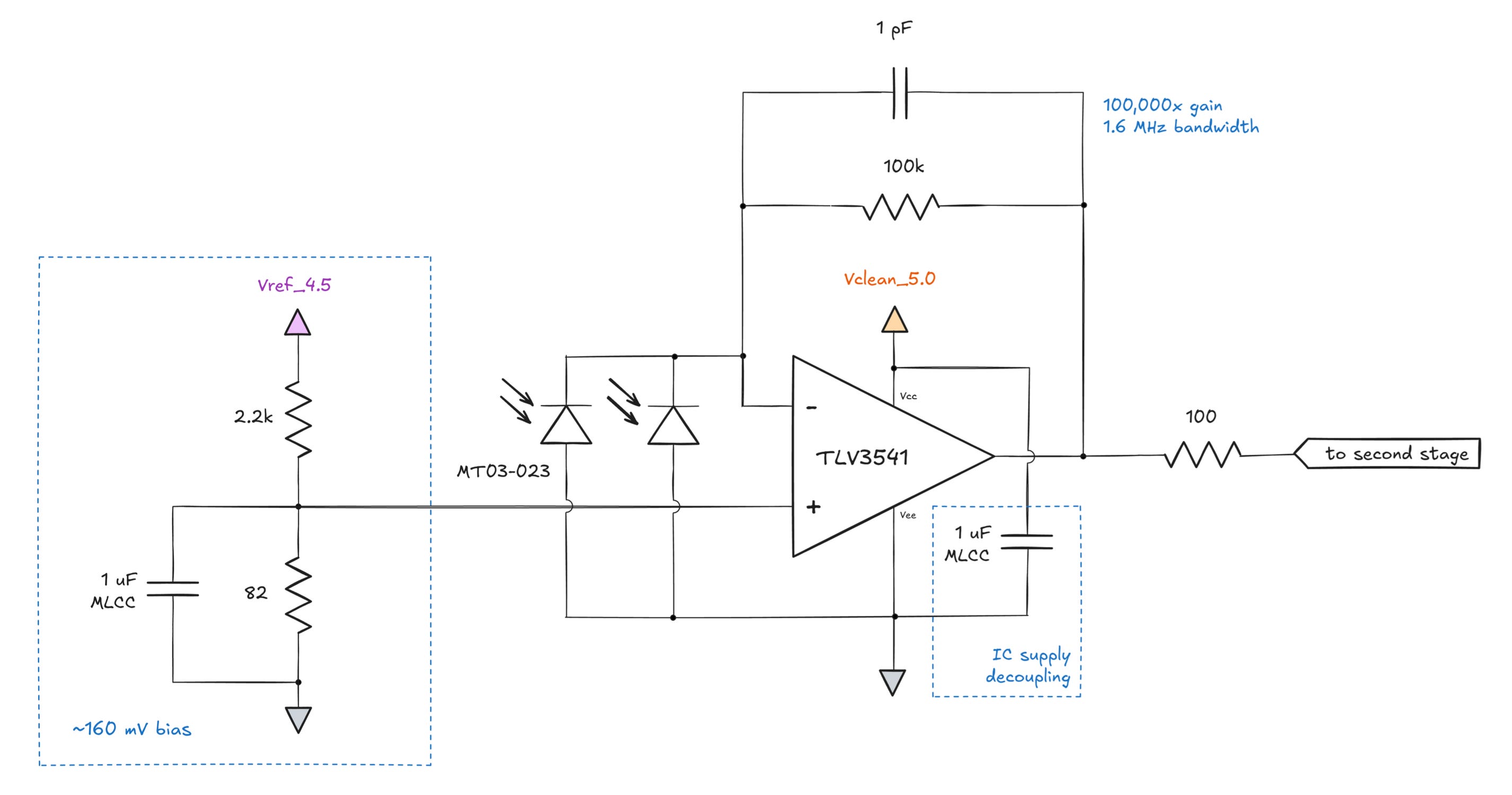
It all started with a pair of Marktech MT03-023 diodes and a textbook transimpedance amplifier. The diodes have an advertised response time of 100 nanoseconds and a capacitance of 20 pF each. The op-amp at the heart of the circuit — TLV345x — is a nifty device with a 100 MHz bandwidth and a 150 V/µs slew rate:
With some allowance for parasitics on the input pin, the maximum cutoff frequency of the amplifier can be calculated the following way:
Because I used a 1 pF feedback capacitor in lieu of the optimal value (0.8 pF), the actual bandwidth is a bit lower, but the difference shouldn’t matter. I was aiming for microsecond-range response times, so 1 MHz was enough.
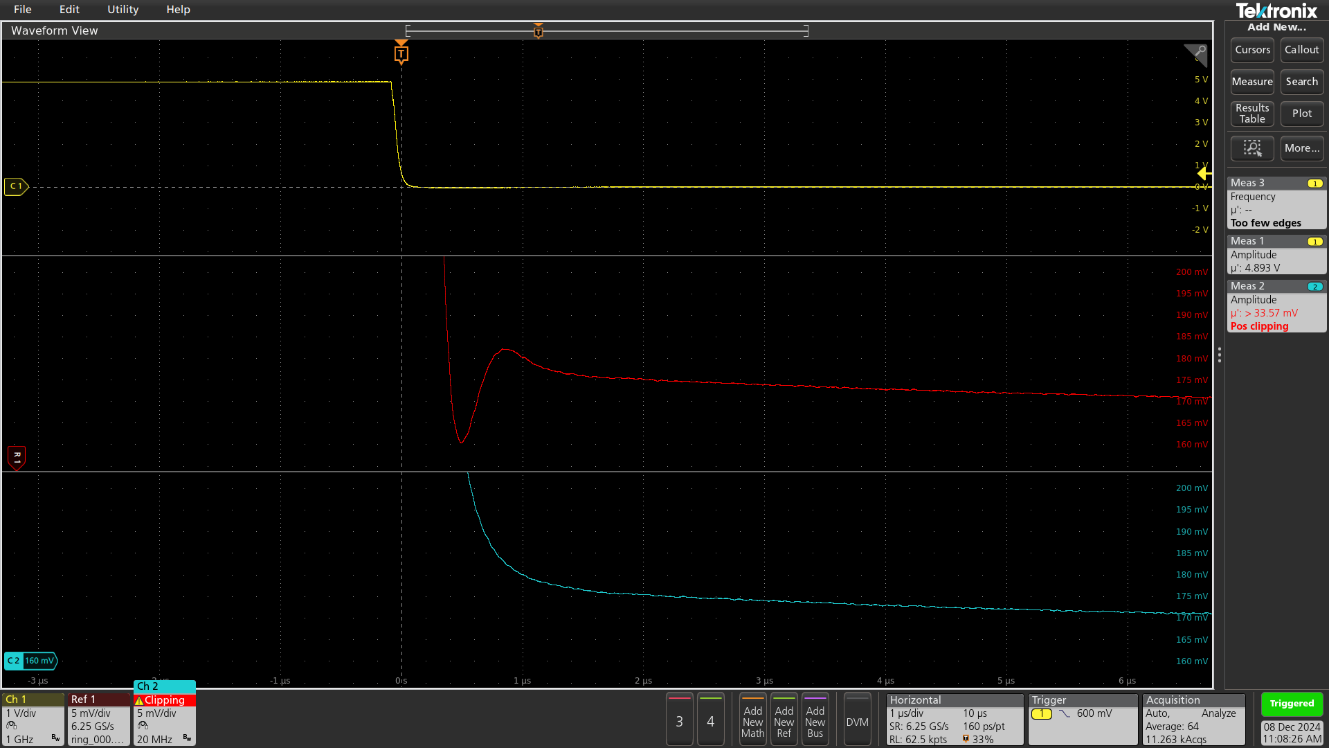
Well, that’s the theory. In practice, the amplifier’s step response looked terrible:

The yellow trace is the signal that’s driving a bunch of LEDs; the blue trace is the output from the photodiode amplifier. Never mind the small amount of ringing ahead of the 1 µs mark: the problem is that the signal takes another 15 µs to reach the steady-state “dark” reading. This drawn-out slope has a vertical span of about 10 mV.
Swing… and miss
I theorized that I must be observing some consequence of the capacitive nature of the photodiode. What sent me down that path is that the timing just made sense: it takes about 18 µs to charge a 40 pF capacitor via a 100 kΩ resistor. But why wasn’t the op-amp doing anything? Who knows — perhaps I was running into some large-signal step response corner case that’s not covered in the chip’s datasheet.
I decided to implement the bootstrapping technique from an earlier post to eliminate the photodiode’s capacitance. Neglecting the 160 mV voltage divider and the supply caps, the new circuit looked like this:

This was a worthwhile modification that eliminated ringing and reduced noise. That said, when the dust settled, I was still staring at the same settling curve — just without the capacitive wobble in front:
The photodiode whodunnit
I experimented aimlessly for a couple of days. I tried replacing the op-amp with a faster chip (OPA356); it made absolutely no difference, so I ruled out the IC as the bottleneck. I tinkered with a lower value of the feedback resistor; this reduced all parts of the signal proportionally, but didn’t shorten the length of the “tail”; so much for the capacitance hypothesis. I even wondered if there’s something phosphorescent in my test environment — perhaps the lens of the LEDs or the photodiode?
At some point, I noticed that the amplitude of the tail was proportional to how long the LEDs stayed on — but the effect tapered off past about 20 µs. The following plot shows the output for LED runtimes of 1 µs, 5 µs, 10 µs, 20 µs, and 40 µs:

I eventually came across an obscure 2013 slide deck from the Lawrence Berkeley National Laboratory that made me realize the culprit is the photodiode — and that for precise signal measurements, the 100 ns response time given by the manufacturer is a bit of a joke.
If you need a recap of how semiconductor junctions generate photocurrent, start here; with that out of the way, let’s have a look at the construction of a generic photodiode:

The device could be made by out of two heavily-doped p-type and n-type materials, but that would make the p-n depletion layer very thin. With an initial abundance of charge carriers on both sides, you don’t need them to diffuse from afar before the internal electric field becomes strong enough to hinder the layer’s growth.
In a photodiode, most of the current is generated when a photon creates an excited electron-hole pair in the depletion region; the region’s internal field then whisks them away in two opposite directions. It follows that to maximize the number of photons absorbed within the depletion layer, you want to make it reasonably thick. That’s why the bulk of the device is made from a lightly-doped n-type substrate: the material has lower charge carrier density, so the formation of the p-n junction involves diffusion across greater distances.
But the interesting part is what happens beneath. If a photon overshoots and is absorbed below the active region, this generates an electron-hole pair that isn’t subject to the depletion layer’s electric field. Normally, in lightly-doped silicon, the pair just sits there for perhaps 10-20 µs before recombining — but if the generation happened near the boundary, either the electron or the hole may randomly diffuse across into the depletion zone. An electron diffusing from the n-side will be ejected back where it belongs; but a hole may get whisked away to the other side, contributing to the net current generated by the photodiode.
The gotcha is that the primary, depletion zone (“drift”) current is pretty much instant: charge carriers start moving right away, and the generation of new ones ends as soon as the influx of photons stops. In contrast, a charge carrier generated right beneath the depletion region may linger there for many microseconds, then randomly wander into the field after the illumination has ceased. This “diffusion” current is small, but takes a comparatively long time to taper off.
This also explains why the magnitude of the effect I’ve been troubleshooting depended on the “LED on” time, but only up to a certain point; for the first twenty microseconds, we’re generating more and more diffusion carriers — but eventually, the system reaches equilibrium where the old ones start recombining just as fast as we’re cranking out new pairs.
So, yep. On the page 44 of the LBNL presentation, you can find the following plot:
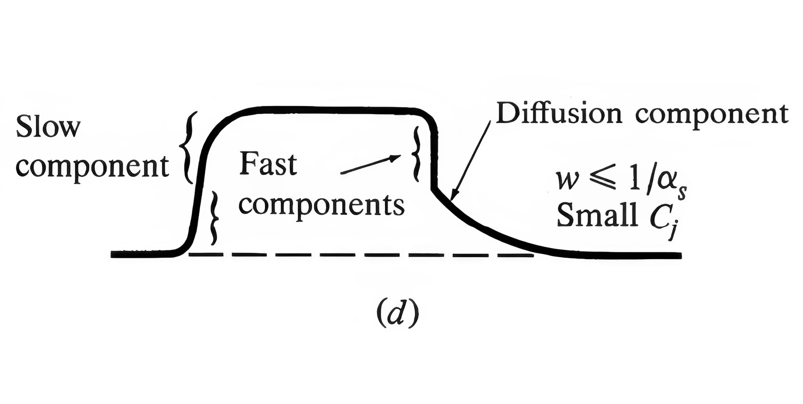
And indeed — at the right zoom level, the knee between the fast response and slow response is easy to see:

Few other online sources talk about this effect. I bet that most people don’t even realize it’s there: when dealing with high-speed signals, sub-1% accuracy is typically not a concern. Conversely, if you’re making precise measurements, you’re almost never in a rush to get the final reading in under 20 µs.
The good news is that the mystery is solved. The bad news is that the phenomenon is intrinsic to the sensor and probably can’t be eliminated with simple electronic trickery. Reverse-biasing the diode widens the depletion region, helping capture more photons where we want them; that said, although even a fairly modest bias flattens the curve to a noticeable extent, it doesn’t make the effect disappear:

One remaining thing I want to try is pulse the reverse-bias voltage to see if the diffusion charge carriers can be “swept up” prior to measurement. If not, then software compensation might be the only way to get the project done.
👉 For a thematic catalog of articles on this site, click here.
I write well-researched, original articles about geek culture, electronic circuit design, and more. If you like the content, please subscribe. It’s increasingly difficult to stay in touch with readers via social media; my typical post on X is shown to less than 5% of my followers and gets a ~0.2% clickthrough rate.
I seem to recall -30V reverse bias in a datasheet, maybe the analog devices one you referred to earlier.
How do you know the LEDs are generating a clean square wave light output when you pulse them for 10 us? I've tried to do something similar to what you're doing (completely different application) and wasn't sure my LEDs were generating clean pulses - if not, the messy photodiode output might be "real". I have been planning to setup a mechanical light chopper (spinning slotted disc) to generate light pulses with known edge characteristics. (Quite possibly you know more about LED physics than I do...)