
What's inside an op-amp?
The internals of operational amplifiers are typically not explained well. Real talk about the differential pair.
In an earlier article on signal amplification, I discussed a couple of basic transistor amplifier circuits and then introduced op-amps as a better-behaved version of the same. This left one question unanswered: what’s inside an op-amp, anyway?
It’s easy to give a superficial answer. A typical operational amplifier has three main parts: a differential input stage, a voltage amplifier, and a push-pull output circuit. We covered the latter two in the previous article, and it’s tempting to wave away the first bit too.
Yet, the differential stage is a pretty interesting animal. At its heart lies an arrangement of transistors known as the differential pair (or “long-tailed pair”), and an accurate explanation of its mechanics is hard to come by. I’ll try to address this below — but let’s start with a brief detour.
The I-V curve of a field effect transistor
Let’s consider a typical n-channel MOSFET. We know that it’s a voltage-controlled device: that is, a voltage signal applied to the gate terminal (Vgs) modulates the flow of current between the two other terminals — drain and the source (Id).
From this description, one could assume that FET is just a variable resistor: a device where the gate voltage dials in a specific drain-source resistance, and where that resistance stays roughly the same no matter what voltage (Vds) appears across the other two terminals. If that model is true, the drain-source I-V plot (Id-Vds) for a given gate voltage should look about the same as it does for a resistor:
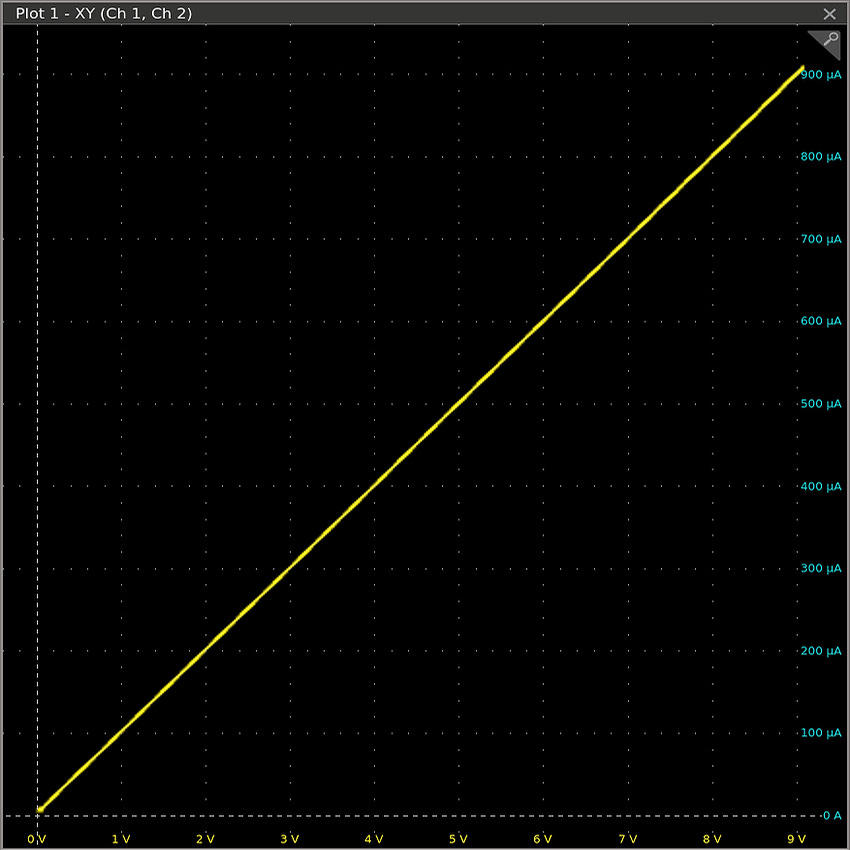
The diagram, captured for a 10 kΩ resistor, makes perfect sense: I = V/R, so if R is constant, the current through a resistive load should be directly proportional the applied voltage.
But that’s not at all what happens with a FET! Don’t take my word for it. I recorded the following curve for a common BS170 transistor at Vgs = 2.25 V. I selected this voltage empirically just to maintain the same scale for both plots:
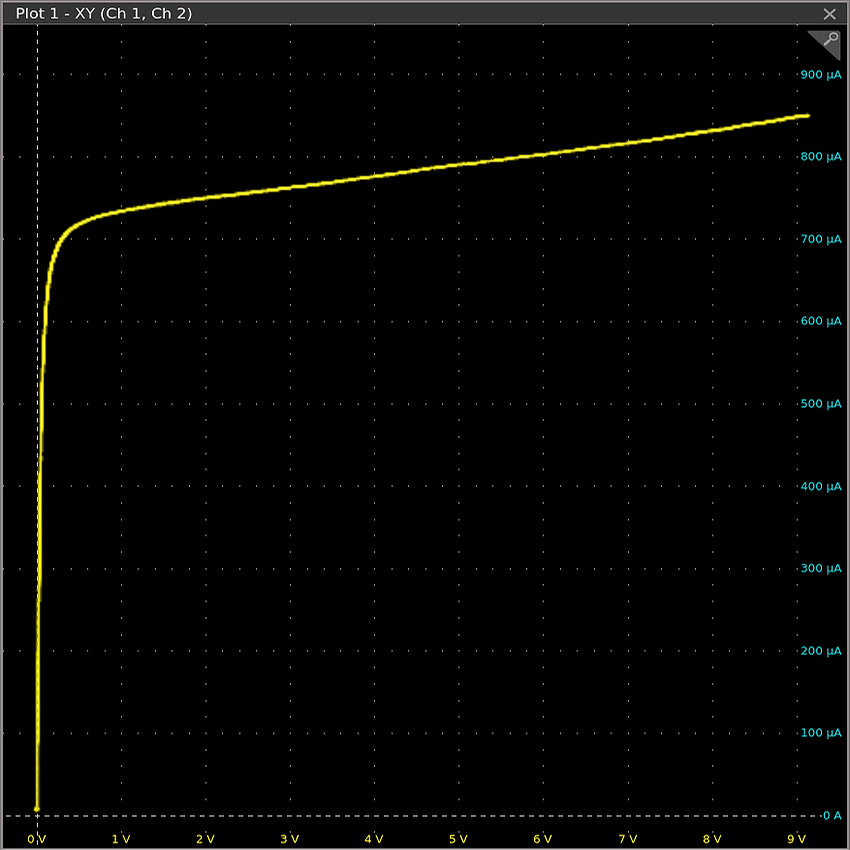
As it turns out, the resistance of a FET is strongly dependent not only on the Vgs input signal, but also on the potential across its drain and source terminals. In particular, for any given Vds past a modest threshold, the transistor appears to be a (nearly) constant-current device. In the plot, the current stays at 800 µA +/- 10% for Vds all the way from 0.5 to 9 V.
The long-tailed pair
Keeping this detail in mind, let’s get back to op-amps. As mentioned earlier, the essential building block of most differential amplifiers is the long-tailed pair; its simplest variant, drawn with n-channel MOSFETs for consistency with the earlier article, looks the following way:
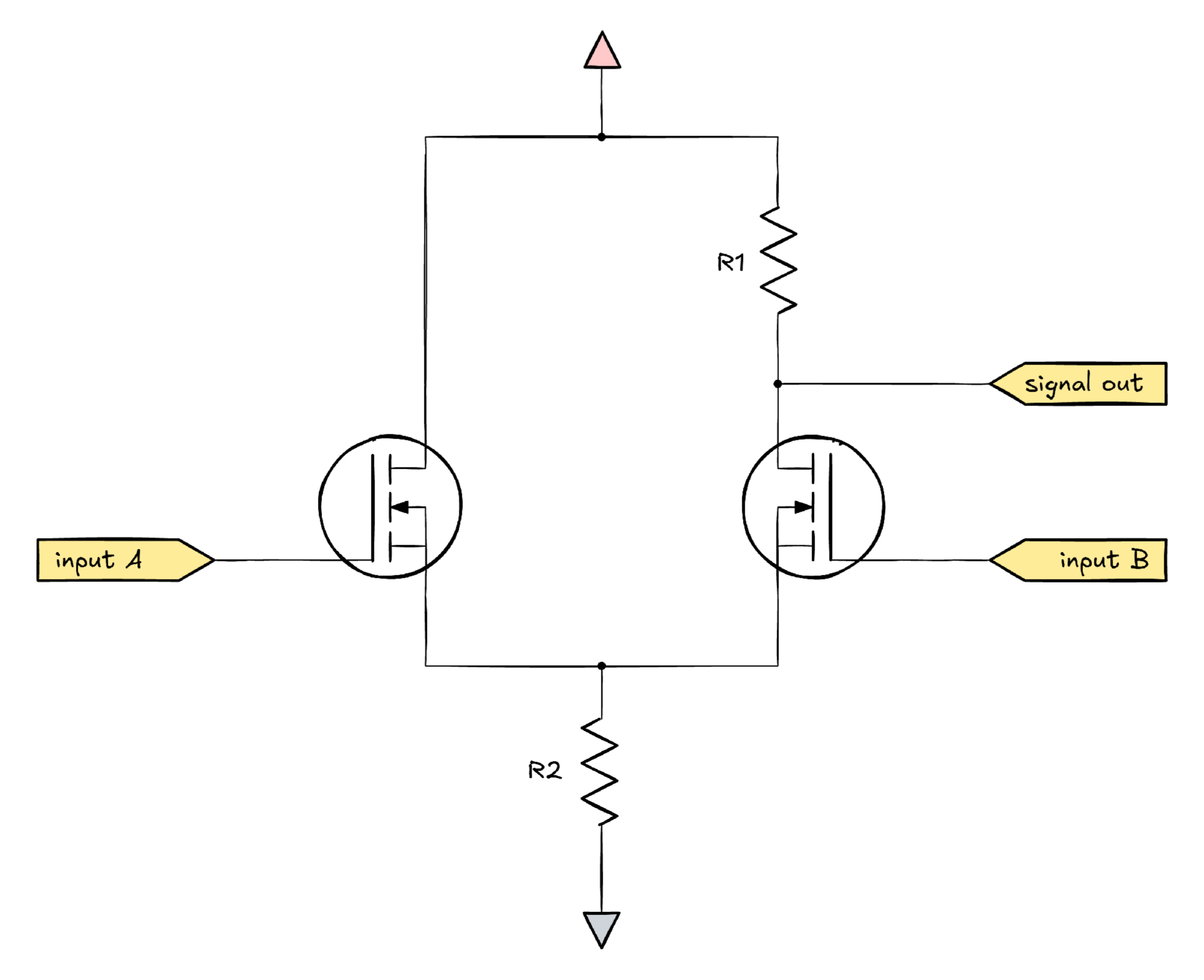
The circuit consists of a pair of voltage followers sharing a common resistor on their low side. Each transistor will conduct only if the voltage on its gate terminal is sufficiently higher than the voltage on the source terminal (Vgs > Vth). Because the flow of current through the transistor causes a voltage to build up across R2, the transistor will admit only as much current as needed for the resistor voltage to reach Vin - Vth.
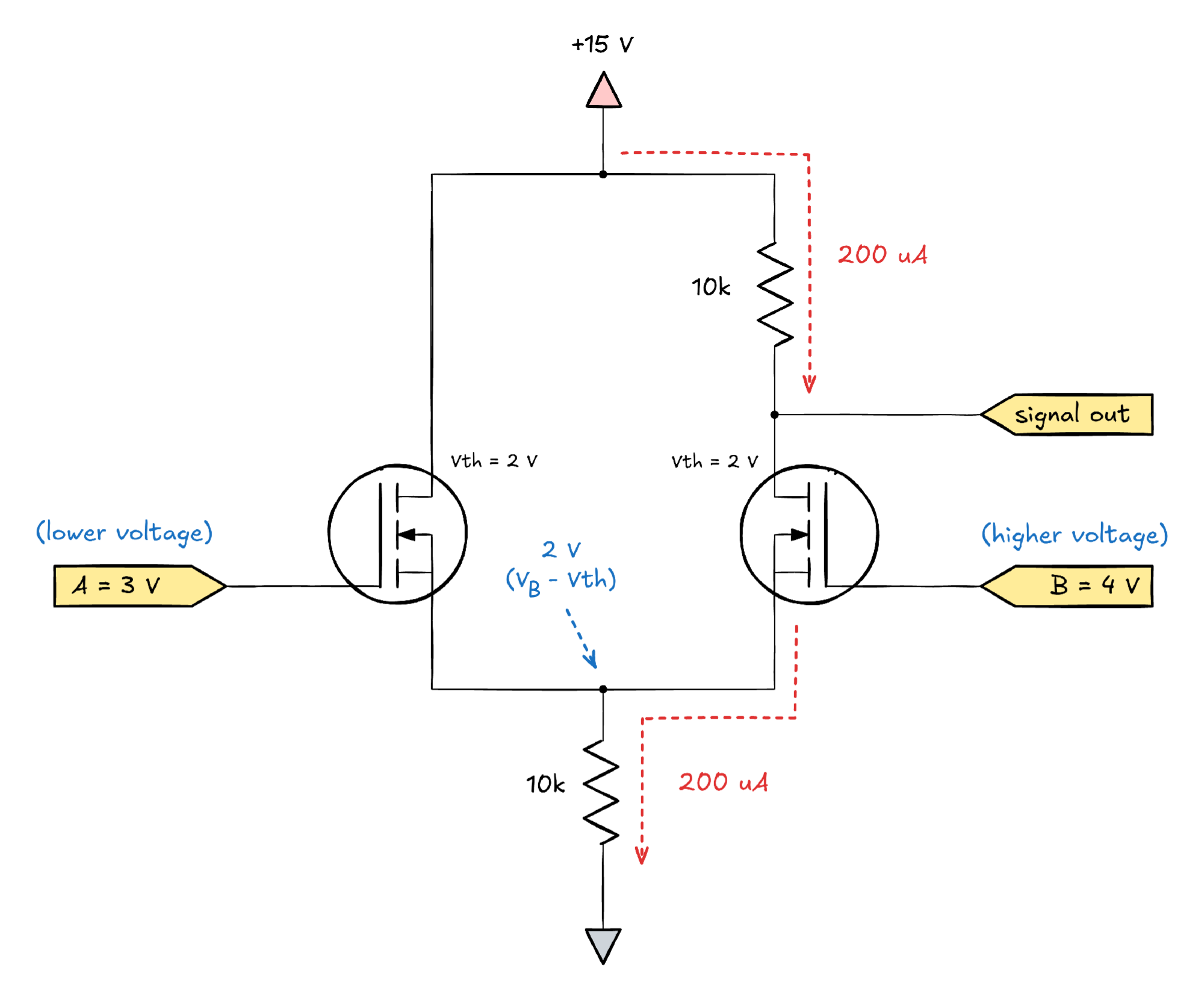
Let’s make a couple of assumptions about component values and voltages and look at what happens if A > B:
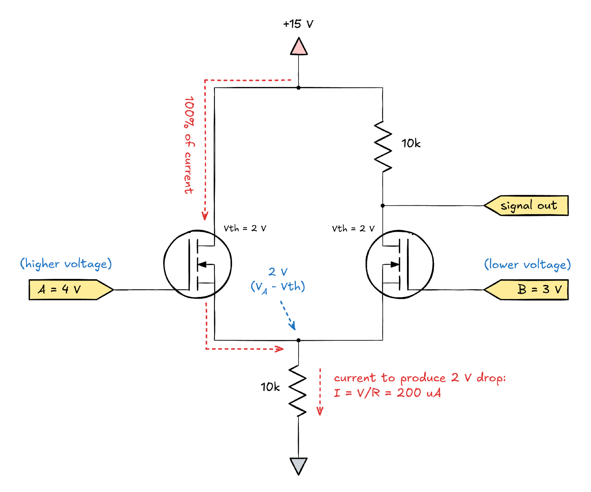
In this scenario, the equilibrium state is a 200 µA current is flowing entirely through the left branch of the circuit; the transistor on the right is not conducting because its source terminal is sitting at 2 V and the gate is only 1 V higher than that (i.e., Vgs < Vth). And because this transistor is off, the voltage at the output node is equal to Vdd.
In the inverse situation (A < B), the branch on the right ends up doing all the work:
Because there is 200 µA flowing through the upper resistor, there is a V = IR = 2 V drop at the output pin; in other words, Vout = 15 V - 2 V = 13 V.
Finally, if A and B are both at 4 V, both branches are handling 50% of the current, so the voltage drop across the upper resistor is halved, putting Vout at 14 V.
At first glance, this might sound like the behavior of an op-amp: we have three distinct output voltages for A < B, A = B, and A > B. Indeed, many online sources try to pass it off as a differential amplifier. That said, the circuit has a fatal flaw: its output voltage doesn’t depend only on the difference between A and B. To illustrate, let’s consider a scenario where A = B, but their common voltage is a bit higher — say, 6 V:
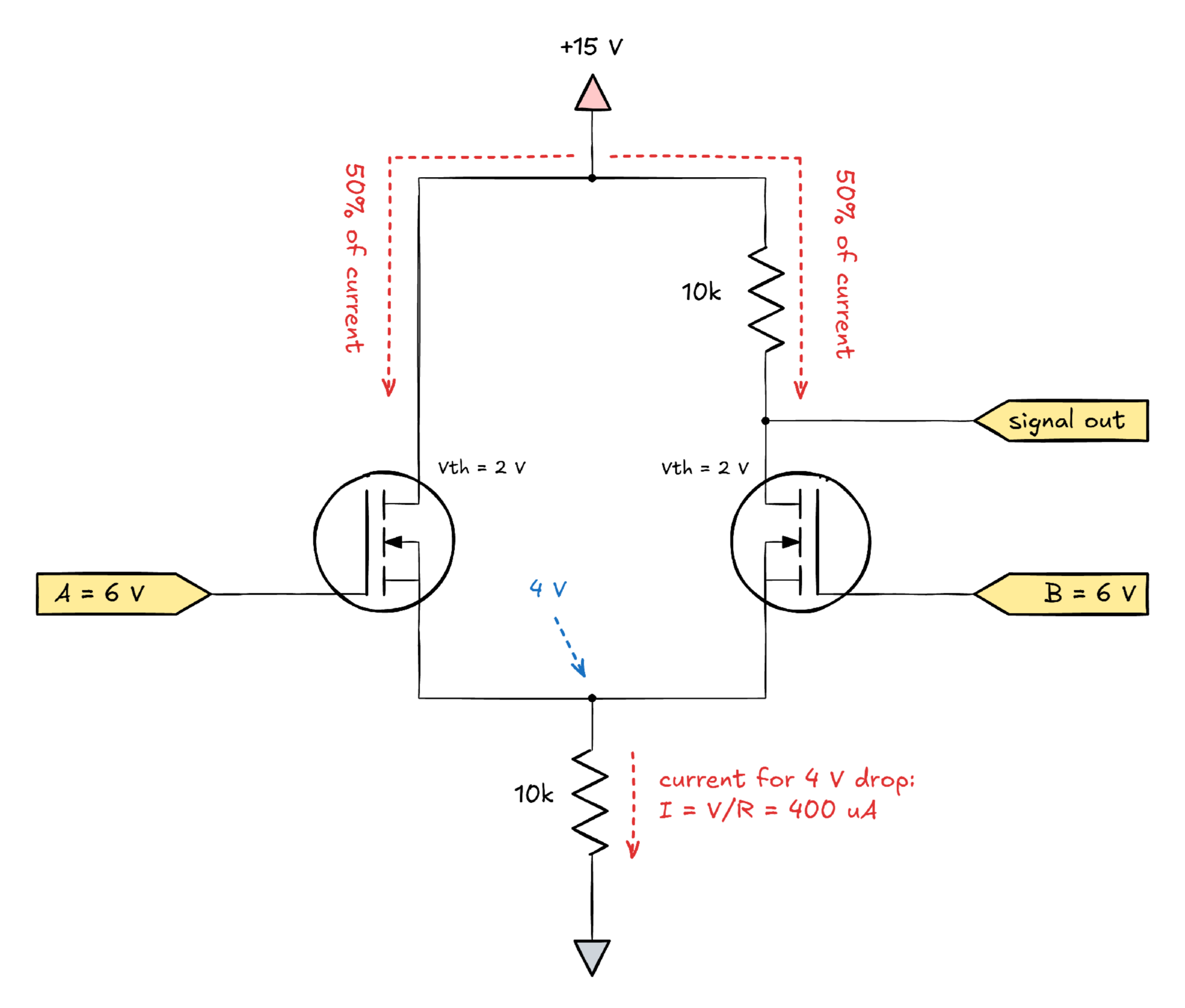
In this scenario, a drop of 4 V needs to develop across the bottom resistor before the transistors reach their cut-off points. This results in a combined current of 400 µA divided equally across both branches. In the right branch, the 50% current (200 µA) causes a 2 V drop across the output resistor, putting Vout at 13 V — exactly the same as in the A < B scenario before!
In other words, the differential amplifier is a dud. It is sensitive to common-mode inputs, making it impossible to reliably distinguish between differential voltages.
A workaround is hinted at by the name of the circuit: it’s called a “long tail” because in order for the amplifier to behave correctly, you need to maintain ample distance between the permissible input voltages and the bottom supply rail. For example, in a 15 V circuit, we could constrain the inputs to a range between 14 and 15 V. This way, a significant voltage drop would always be present across the “tail” resistor, and the overall current would vary only a tiny bit — making it easy to distinguish between 0%, 50%, and 100%.
Toward a shorter-tailed pair
Of course, this input constraint is rather severe, especially in the age of single-supply electronics that commonly run off as little as 3.3 volts.
To improve this circuit without sacrificing its input range, it would be necessary to replace R2 with a device that can recreate a wide range of voltage drops while requiring only fairly modest current swings. This would make the current flowing R1 fairly insensitive to any common-mode artifacts.
Well — that’s our cue to wheel out the previously-discussed FET I-V curve:
As seen in the graph, a spectrum of voltage drops ranging from 0.5 to 9 V (x scale) can be created by varying current by as little as +/- 10% (y scale).
A single FET with a carefully trimmed gate voltage could be used as a drop-in replacement for R2. That said, its characteristics will drift in response to factors such as ambient temperature, so it’s best to add some sort of a feedback loop. One such circuit — known as the current mirror — is shown below:
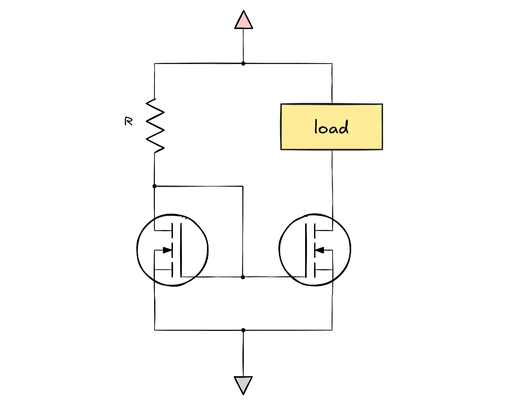
For a moment, let’s focus only on the part on the left. At first, there’s no current flowing through the transistor, so the drain terminal quickly shoots toward Vdd; so does the gate terminal, prompting the transistor to start conducting. This, in turn, creates a voltage drop across R, eventually lowering the gate voltage toward the cut-off region. This is a negative feedback loop; an equilibrium is reached when the transistor is admitting current equal to I = (Vdd - Vth) / R.
On its own, this is worthless, but there is a carefully matched transistor on the right. It has no feedback mechanism, but is supplied with the same gate voltage — and therefore, should admit the same current through the connected load, with relatively little dependence on what the load is.
This particular current mirror is controlled by a fixed reference — R — so it becomes what’s known as a “current source”. This term is somewhat sketchy because the device does not move any electrons on its own, not in the sense that a battery does; rather, it’s just a current-limiting contraption. But I digress.
Current sources have their own (uncommon) circuit symbol, so a revised version of the not-so-long-tailed pair might look this way:
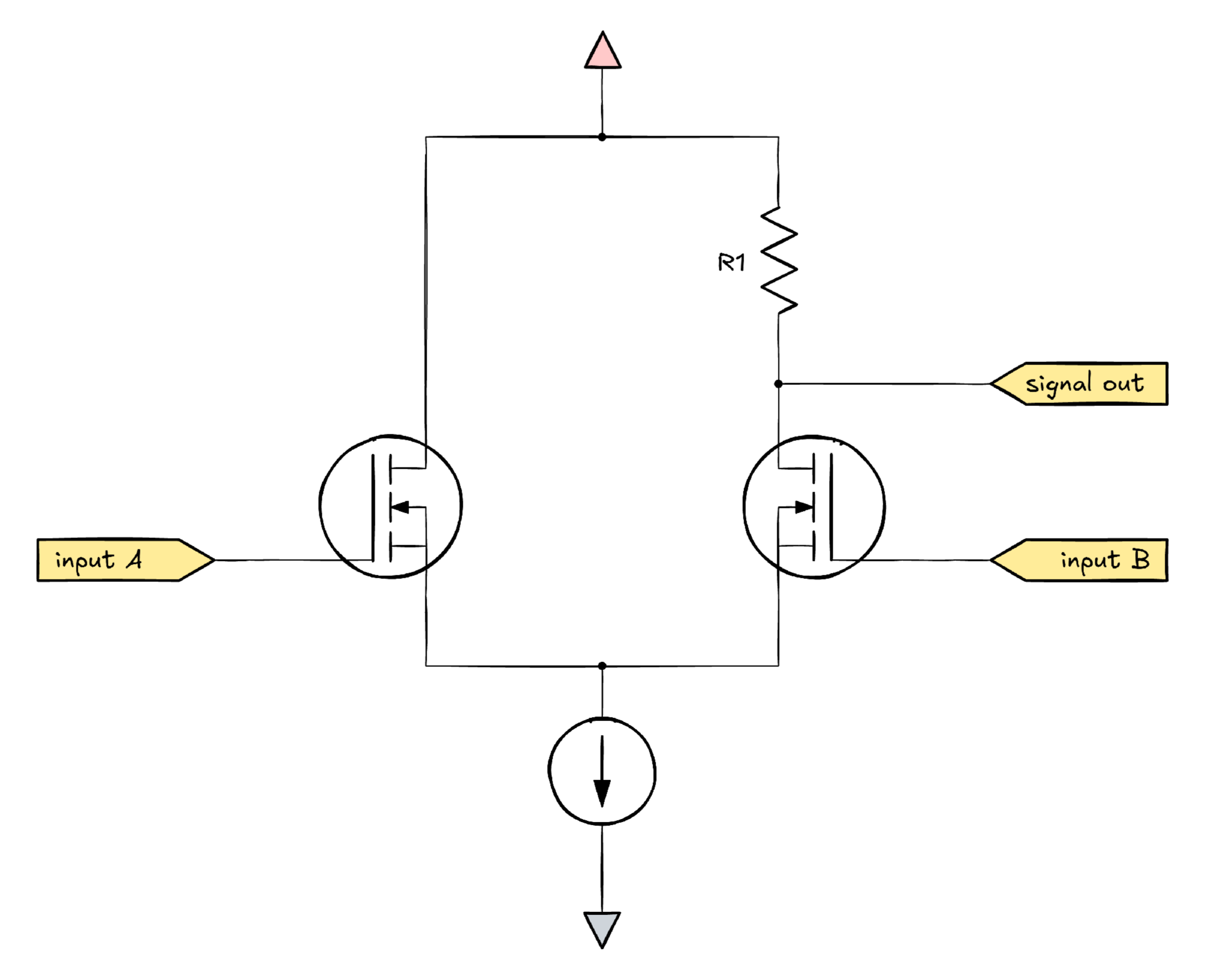
And that, in a nutshell, is a very basic but reasonably well-behaved differential stage.
Because the Vgs < Vth dead zone near 0 V is typically undesirable, the circuit is often constructed as an upside-down version with p-channel MOSFETs. It’s also possible to employ JFET transistors to get rid of the threshold altogether. In all cases, the operating principle is the same.
👉 To review the entire series of articles on analog and digital electronics, check out this page.
I write well-researched, original articles about geek culture, electronic circuit design, algorithms, and more. This day and age, it’s increasingly difficult to reach willing readers via social media and search. If you like the content, please subscribe!
Minor nitpick: The arrow in the current source symbol represents the direction of current flow. The second long-tailed pair diagram has it the wrong way around.