
The basics of decoupling capacitors
How to stabilize digital supply voltages - and why most of the online advice on this topic is suspect.
Two decades ago, to build a portable music player, you had to clobber together several hundred electronic components. Today, you can accomplish the same with a single chip and a dozen passives. Heck, you might even get Wi-Fi and Bluetooth for free.
One of the few discrete components that survive and thrive in the face of growing integration is the humble decoupling capacitor. It’s not just that the device is hard to manufacture on the die of an integrated circuit; in the world high data speeds and low supply voltages, it has an increasingly important role to play in keeping the circuits humming along.
Among hobbyists, the understanding of decoupling caps continues to be hit-and-miss. Some folks skip them altogether and live to tell; others follow ancient lore of uncertain origins, producing monstrosities such as this:


In this article, I’m hoping to cast some light on the actual role of decoupling capacitors in digital circuits — and to offer advice on how to integrate them into your designs without going overboard.
What does a decoupling capacitor do, anyway?
In a steady state, a typical CMOS integrated circuit needs very little power. The chip’s energy consumption is associated predominantly with state transitions — that is, toggling between “zero” and “one”. That’s because the process requires moving electrons back and forth to charge or discharge the gates of field effect transistors inside the chip.
Some internal state transitions require relatively little current, but others are more demanding; this is particularly true for the operation of larger transistors that drive output lines. To toggle them at megahertz speeds — a task that demands rapid rise and fall times — the chip must momentarily source significant currents. In a typical microcontroller, the transition usually takes no more than several nanoseconds, but may involve hundreds of milliamps.
This poses a challenge. At high and rapidly varying currents, PCB traces exhibit resistive losses and non-trivial inductive reactance. The imperfect demand response characteristics of the power supply also get in the way. In the end, even seemingly minor digital switching can cause significant voltage fluctuations and electrical noise across the entire circuit.
The following oscilloscope plot shows the effects of a very unassuming ATmega microcontroller repeatedly toggling a couple of unconnected output pins. MCU clock speed is 8 MHz; square wave rise time is somewhere in the ballpark of 5 ns:
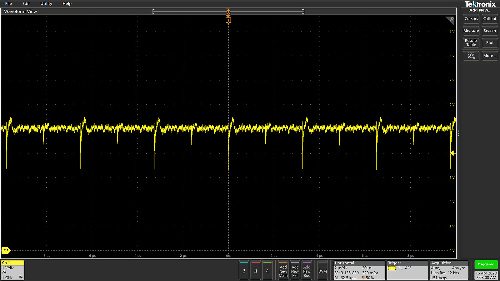
The peak-to-peak amplitude of this noise, as sampled at the MCU supply pins, is almost 2 volts — about 40% of the nominal supply voltage. This in itself can be enough to destabilize the MCU. Just as important, because the chip no longer has a stable Vdd and GND reference shared with other parts of the circuit, interfacing it to other devices might prove difficult. It’s not that this setup is bound to malfunction, but unexplained and hard-to-diagnose issues can creep up with ease.
This brings us to the purpose of decoupling capacitors: they are placed across the voltage supply lines and physically close to the offending chip to handle switching transients while preventing high currents and minimizing voltage fluctuations in other parts of the circuitry.
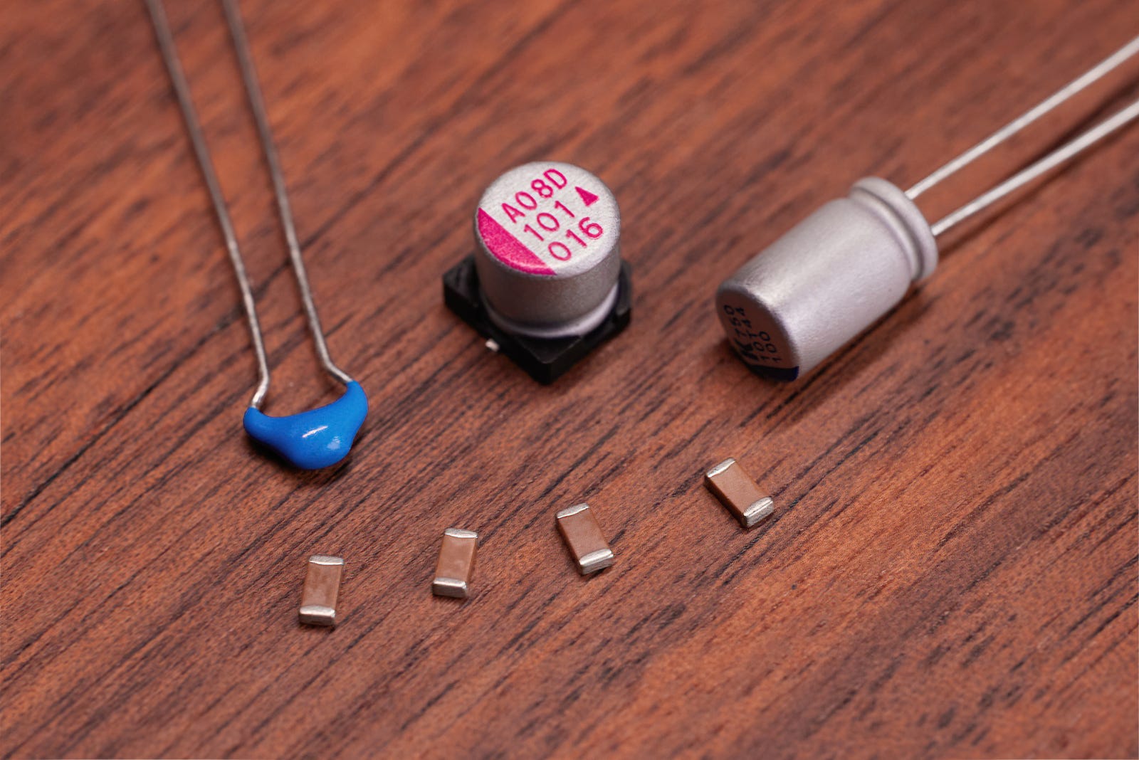
To do this, the capacitors must have low equivalent series resistance (i.e., be able to charge and discharge quickly); for this reason, multilayer ceramics (MLCCs) should be used instead of the comparatively sluggish electrolytic caps. But above all, to work effectively, the capacitors must be as close as practical to the chip’s supply pins, so that board parasitics don’t get in the way. The following oscilloscope trace captured for another mildly noisy 8-bit MCU illustrates the point:
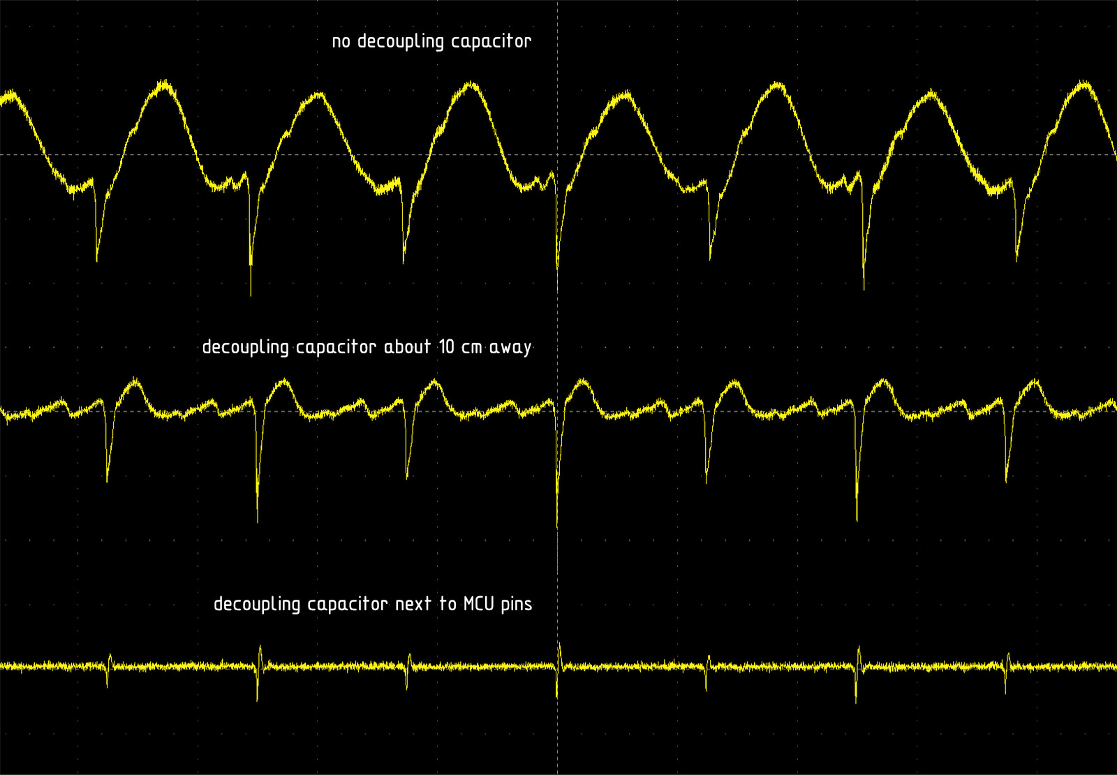
One could analyze the setup in terms of a lowpass filter formed in tandem with upstream and downstream impedances, but these parameters are hard to faithfully estimate. Most of the time, we go by rules of thumb: a single 100 nF to 1 µF MLCC per supply domain, operated well clear of its maximum voltage, is typically enough to deal with all intrinsic switching currents of PIC, AVR, or mid-range ARM microcontrollers. Your life gets more complicated in the gigahertz territory, but in hobby work, this is seldom a concern.
As a side note, the caveat about staying clear of the capacitor’s maximum voltage has to do with a peculiar quirk of multilayer ceramic capacitors: their rated capacitance is given for operation with DC bias across the terminals; as the bias approaches the maximum rated voltage, the value can drop by as much as 60-80%:

In decoupling applications, MLCCs are always used with a DC bias — so if you need to hit a specific number, you should either use a capacitor with voltage headroom (e.g., a 16 V cap in a 3.3 V circuit), or look for a higher rated capacitance to make up for the loss.
(I have a followup article about this phenomenon here.)
In any case: beyond this baseline recommendation, additional “bulk” capacitance might be appropriate if the MCU is driving substantial loads that may produce less sudden but longer-lived voltage sags. This can be accomplished with a single larger MLCC (e.g., 10 µF); with several identical, small MLCCs in parallel; or with a small fast-acting MLCC coupled with a larger but slower aluminum-polymer cap (10-100 µF). In the latter configuration, the larger capacitor can be safely placed some distance away.
Is a capacitor always enough?
A well-chosen decoupling capacitor can greatly reduce switching noise, but the component has a finite capacitance and a non-zero impedance. The capacitor’s impedance increases not only toward DC, but also toward very high frequencies; this is because of the fairly large, conductive surface area inside the device that forms a small inductor and limits the capacitor’s response speed. The end result is that a typical MLCC can’t supply high currents at (sine wave) frequencies above 100 MHz or so. The AC specs are worse for larger components, so a 0402 MLCC will outperform a 1206 cap.
Either way, some attenuated high-frequency noise will inevitably get through — and while adding extra capacitors can offer some modest improvement, the strategy has diminishing returns.
In sensitive circuits, the problem of this residual high-frequency noise can be further mitigated by placing a small ferrite bead in series with the supply and ahead of the decoupling caps. The inductor provides a low impedance path (few milliohms) for DC signals while impeding megahertz-range AC much better than a shunt capacitor to the ground can — usually performing well to 1 GHz or so, at which point parasitics once again get in the way.
The following example from the spec for SAM S70 MCUs, recommending the use of two beads with an impedance of 470 Ω at 100 MHz on the supply lines for the USB transceiver and the phase-locked loop (PLL) clock multiplier:

Combined with decoupling capacitors, the setup works remarkably well:
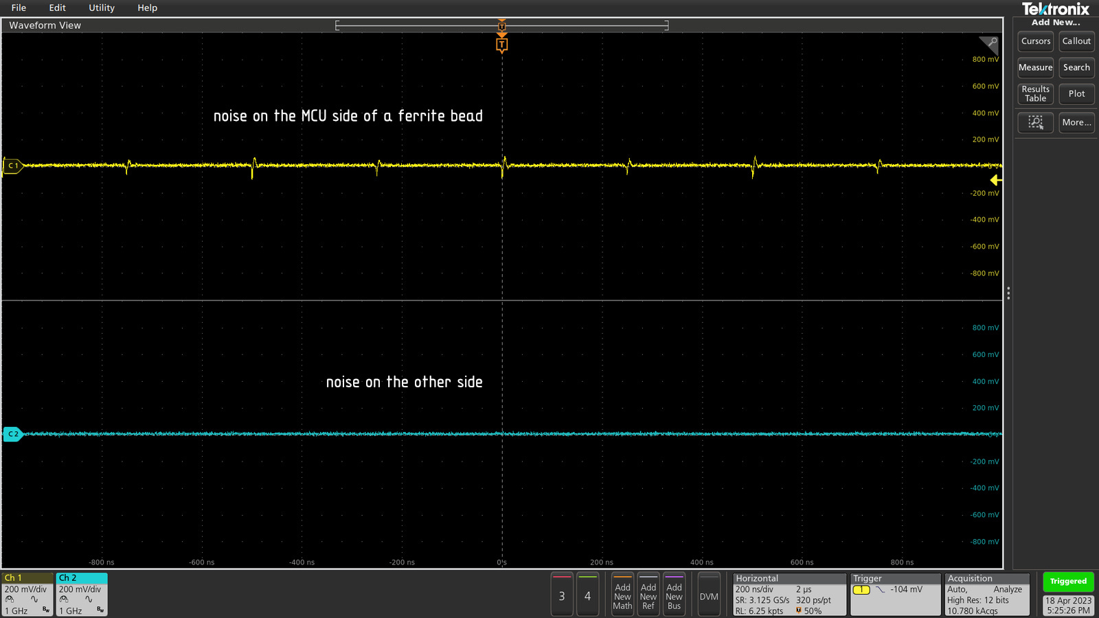
That said, it must be underscored that a ferrite bead doesn’t eliminate noise; it merely contains it to the side it originated from. It can shield analog circuitry from digital switching artifacts, or it can protect the MCU from noise originating elsewhere; in all cases, it must be followed by a decoupling capacitor to provide some power reserve for downstream circuitry. An upstream (supply-side) capacitor is wise, too.
A related trick is to put small ferrite beads upstream on select MCU output lines; this takes the edge off fast-rising square wave signals, and can reduce needless currents and spurious radio frequency emissions when a high-speed microcontroller is driving slower buses such as I²C or SPI. In a pinch, small resistors might also do, although the setup will typically perform worse.
With this out of the way, most other noise mitigation techniques tend to revolve around board design. For example, keeping sensitive analog circuitry at an arm’s length from digital signals is a good PCB layout strategy; so is placing an unbroken ground plane immediately under high-speed data lines to avoid forming large current loops that radiate wideband noise into the open space. (For a separate article on this topic, click here.)
What if the manufacturer says…
The datasheets for some digital chips will outline a suggested way of decoupling them. These recommendations should not be ignored, but are not to be taken as gospel. The manufacturer is trying to cover a variety of extremes, including:
Circuits operated at the lowest permissible supply voltage,
Devices running at the maximum supported clock speed,
Peak utilization of on-chip peripherals,
The customer using the worst decoupling capacitors money can buy (e.g., the "Y5V” variety that loses most of its rated capacitance when operated at an elevated temperature).
Further, the manufacturer is making assumptions about customers’ design preferences. A typical 100 nF MLCC costs about $0.004 a piece in US retail; in contrast, a 10 µF aluminum-polymer cap is about $0.15. A customer doing robotic assembly might favor a dozen MLCCs in lieu of a single MLCC paired with a polymer capacitor. A hobbyist soldering by hand might not.
Instead of blindly following the spec — a practice that still doesn’t guarantee success — it can more useful to validate your design in three ways:
Examine circuit supply noise under normal operating conditions. If the peaks exceed maximum permissible supply ripple, minimum supply voltage, or maximum supply voltage for the digital components, or if switching noise propagates to sensitive analog circuitry, you should improve the design.
If relevant in your project, confirm that signals on any high-speed output busses (e.g., USB) look correct, especially in terms of expected rise and fall times, noise, and any periodic glitches. Oscilloscope “eye diagrams” can help.
As a final test, you can observe the circuit with IC supply voltage reduced 10-20% from the design range. If the digital circuitry continues to operate correctly, you likely have a good safety margin when it comes to switching noise.
What about the “1 nF / 10 nF / 100 nF” rule?
There is this old adage that for optimal decoupling, you must combine two or three capacitors, one or two decades (orders of magnitude) apart. The exact progression of recommended values changes from one oral account to another, but the bottom line is that if you don’t heed the warning, some terrible fate awaits.
The advice made some sense back when each of these capacitors would be made in a different technology. The lowest capacitance would be ceramic, offering low impedance but not packing enough punch to smooth out longer-lasting flukes; the middle cap could be tantalum, offering balanced performance but not excelling in any dimension; and the last one would be aluminum electrolytic, delivering poor high-frequency response but storing quite a bit of juice.
Today, low-cost MLCCs combine high capacitance and low impedance across a wide range of frequencies, so there’s usually little to be gained by playing such tricks. For hobby uses, a single MLCC per each functionally distinct digital voltage supply line is almost always enough.
It is true that at very high frequencies — hundreds of megahertz — the capacitor’s residual inductance becomes a limiting factor. At that point, combining multiple different capacitors can offer somewhat better wideband noise suppression at the expense of potentially creating undesirable anti-resonance peaks in the system (rendering it ineffective at dealing with a handful of specific frequencies). That said, a simpler solution with fewer side effects is to use a specialized low-inductance (feedthrough) MLCC.
What about PCB layout?
As discussed earlier on, it’s important to keep decoupling capacitors reasonably close to integrated circuits; the resistance and inductance of long traces prevents the caps from doing their job. As a rule of thumb, keep the distance under 1-2 cm whenever practical. You typically have more leeway with slow 8-bit MCUs, and less with high-performance 32-bit chips.
On the flip side, it’s best not to get sidetracked with more exotic advice found on the internet. One persistent claim is that the layout on the left is dramatically better than the one on the right:

As the story goes, in the first circuit, voltage spikes reach the capacitor first, allowing it to kick in before the noise “spills over” onto the supply lines. In the second layout, the capacitor is supposedly reached too late. Don’t get me wrong: signal propagation speeds sometimes need to be taken into account in PCB design. That said, across such tiny distances, it doesn’t matter unless you’re working with multi-gigahertz signals — and in that frequency range, your standard MLCC isn’t of much help.
👉 For an addendum on the frequency-domain treatment of square wave digital signals, see this article. For more articles about electronics, visit this index page.
I write well-researched, original articles about geek culture, electronic circuit design, algorithms, and more. This day and age, it’s increasingly difficult to reach willing readers via social media and search. If you like the content, please subscribe!
It is probably worthwhile to include a brief discussion of the three-letter MLCC capacitor codes. In essence, they divide the capacitors into three classes:
1) Thermally-compensated, showing negligible capacitance change across a wide range of operating temperatures. A common example is C0G.
2) Thermally-stable, showing fairly modest temperature dependency, usually with a deviation around +/- 15%. These are much cheaper and are usually good enough. A popular example is X5R and X7R.
3) Atrocious, with wild capacitance variations depending on operating temperature, often exceeding +/- 80%. An example is Y5V.
These designations are also somewhat loosely correlated with how the capacitance changes as the DC bias voltage approaches the capacitor's rated maximum. There are no hard-and-fast rules, but in general, Y5V will be a lot worse than C0G.
You may wish to add new design thoughts with using balanced (X2Y.com) capacitors which have a referential third lead and can be self tunable.