
DACs and ADCs, or there and back again
A look at how digital-to-analog and analog-to-digital converters work - from resistor ladders to delta-sigma modulation.
In one of the earlier articles, I remarked that microcontrollers are eating the world. Even for rudimentary tasks, such as blinking a LED, a microcontroller is now cheaper and simpler to use than an oscillator circuit built with discrete components — or implemented using the once-ubiquitous 555 timer chip.
But in this increasingly software-defined world, zeroes and ones don’t always cut it. Image sensors record light intensity as a range of analog values; a speaker playing back music must move its diaphragm to positions other than “fully in” and “fully out”. In the end, almost every non-trivial digital circuit needs specialized digital-to-analog and analog-to-digital converters to interface with the physical world. These devices are often baked onto the die of the microcontroller, but they are still worth learning about.
Simple digital-to-analog converters (DACs)
The conversion of digital signals to analog usually boils down to taking a binary number of a certain bit length and then mapping subsequent integer values to a range of quantized output voltages. For example, for a 4-bit DAC, there are 16 possible output voltages, so its model behavior could be:
0000 (0)  = 0 V
0001 (1)  = 1/15 Vdd
0010 (2)  = 2/15 Vdd
0011 (3)  = 3/15 Vdd
...
1111 (15) = Vdd
About the simplest practical way to implement such a conversion is a resistor-based binary-weighted DAC:
It should be evident that if the binary input is 0000, the analog output is 0 V; conversely, if the input is 1111, the output must be Vdd. For inputs in between, we should get a resistor-weighted average, with each bit having half the influence of its more significant predecessor. This intuitively aligns with how binary numbers work.
We can analyze the behavior a bit more rigorously, too. Let’s see what happens it the input value is 0001. In this scenario, the top three resistors (bits #1, #2, and #3) are connected to the ground in parallel, so we can consider them equivalent to a single resistance:
The bottom resistor for the least significant bit (LSB) connected to Vdd. In effect, the circuit can be thought of as a pair of series resistors forming a voltage divider between Vdd and ground. The output of this divider is:
Analogously, if the input is 1110 (decimal 14), we get Vout ≈ 14/15 Vdd. That tracks with the behavior we were hoping to see.
The most significant issue with this DAC architecture is that the required resistor values quickly get impractical. To avoid high idle currents, the resistance attached to the most significant bit (MSB) can’t be too low; 1 kΩ is a sensible starting point. But then, for a basic 16-bit DAC, this puts the LSB resistor at 1 kΩ * 215 ≈ 32 MΩ; for 24-bit resolution, we’d need tens of gigaohms. Precise resistances of this magnitude are difficult to manufacture on the die of an integrated circuit — doubly so if they need to have the same temperature coefficients.
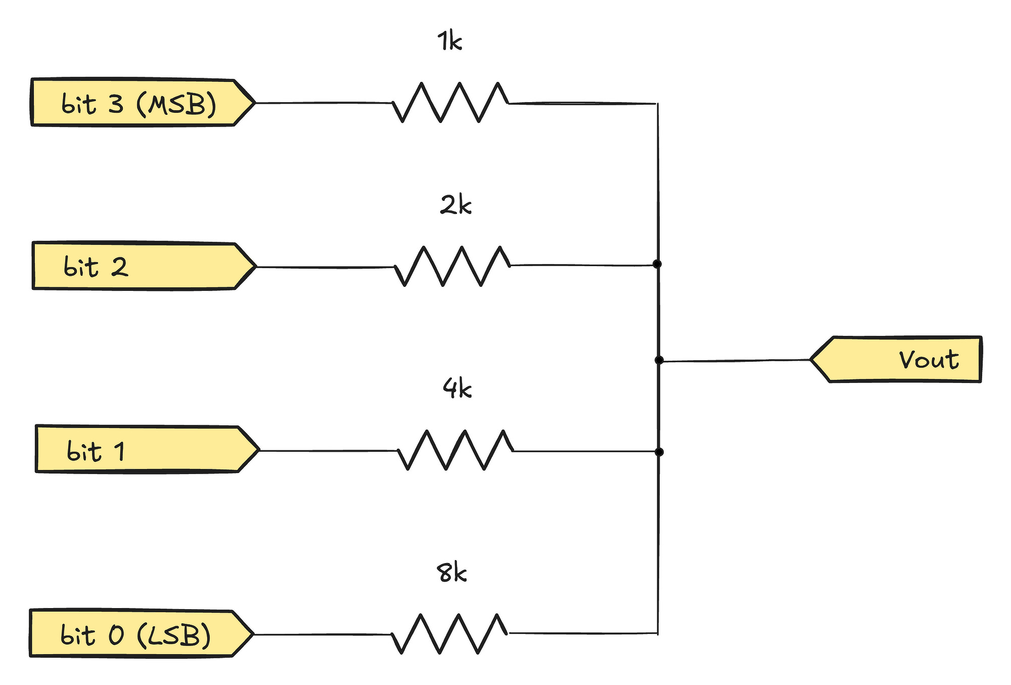
A clever workaround for this issue is the R-2R DAC architecture:

This circuit is less intuitive than its predecessor, but it works in a similar way. To decipher the design, let’s start with the section at the bottom — the two horizontally-placed resistors for bit #0. They supply equal currents to the remainder of the circuit, so we can treat them as functionally equivalent to a single 1 kΩ that’s connected to some synthetic, combined input voltage. This voltage is equal to 0 V if LSB = 0; and to Vdd/2 if LSB = 1. In other words, we have a synthetic input signal equal to 50% of the value for bit #0.
If we make this substitution, we end up with the circuit shown below on the left. Further, because the bottom part now features two 1 kΩ resistors in series (red), it’s equivalent to the 2 kΩ single-resistor variant on the right:

Notice that the situation for bit #1 on the new schematic is analogous to the original analysis we performed for bit #0. The bottom now features a 2 kΩ resistor connected to the corresponding binary input, plus a 2 kΩ resistor feeding from the previously-derived synthetic voltage. In effect, we get a 50% mix of both signals; no matter what’s going on above, we can substitute this portion with a single 1 kΩ hooked up to a yet another synthetic input signal:

This process can continue; it should be clear that after the final iteration, we’re bound to end up with an output voltage that’s 50% of bit #3, 25% of bit #2, 12.5% of bit #1, and 6.25% of bit #0.
(This doesn’t sum up to 100% because some of the upper range is lost to the initial pull-down resistor at the bottom of the ladder.)
Oversampling DACs
Although the designs discussed above are simple and sweet, they also pose challenges with linearity at higher resolutions — especially past 10-12 bits. Resistors can be easily made with accuracy as good as 0.1%, but in a 16-bit DAC, the influence of the LSB is supposed to be just 0.003% of MSB. If the MSB resistor deviates by 0.1% from the intended value, this is more than enough to throw the whole scheme badly out of whack.
This problem led to the development of the so-called oversampling averaging DACs. Such devices output lower-resolution but alternating signals at a high frequency. Then, a lowpass filter on the output averages the values to produce a greater range of slower-changing intermediate voltages.
To illustrate, averaging four subsequent one-bit DAC outputs can add three intermediate voltages in between what the DAC can natively produce — an effective gain of two bits:
average(0, 0, 0, 0) = 0
average(0, 0, 0, 1) = 0.25
average(0, 1, 0, 1) = 0.5
average(0, 1, 1, 1) = 0.75
average(1, 1, 1, 1) = 1
There is a price to pay, of course; for one, some of the high-frequency noise inevitably gets past the filter. That said, the approach is generally pretty robust. Indeed, many DACs used in consumer audio employ single-bit pulse trains at hundreds of kilohertz to produce claimed output resolutions of up to 24 bits. In practice, the noise floor in the circuit typically makes that number fairly meaningless; still, the linearity of 1-bit DACs is superb, because accurate timing is much easier than manufacturing ultra-precise resistors.
Classical analog-to-digital converters (ADCs)
Compared to going the other way round, converting analog voltages to binary numbers is a fairly involved affair. About the only practical way to obtain accurate and instant readings is to use one voltage comparator (an open-loop op-amp) per every quantization level desired, for example:

Such “flash” ADCs are sometimes used in specialized applications where speed is paramount, but the size of the circuit grows exponentially with the number of bits — and with it, the chip’s power consumption, input capacitance, and so forth. For these reasons, they’re usually not made for resolutions higher than 4-8 bits.
A more common architecture is to use a single comparator combined with a reference voltage that changes over time in some predictable way; a rudimentary example may be a capacitor that is being charged through a resistor. The time elapsed from the beginning of the charging process to the comparator triggering can be used to infer the unknown input voltage.
In practice, because the constant-voltage charging curve of a capacitor is nonlinear, the reference signal is more commonly provided by an integrator circuit:

An integrator is a basic op-amp design with an interesting tweak: a capacitor goes where a feedback resistor would normally be. If the voltage on the inverting (Vin-) input becomes higher than on the non-inverting one (Vin+), the output immediately swings lower, allowing some capacitor-charging current to flow via R.
Importantly, this feedback mechanism seeks to keep Vin- near Vin+ — so from Ohm’s law, for a given input voltage and a fixed input resistance, the charging current is constant and is governed just by the value of R. Further, in a constant-current scenario, capacitor voltage ramps up linearly; if supplied with a square waveform, the integrator will output a nearly-perfect triangle wave — a superbly linear reference for an ADC!
The time elapsed between the beginning of the charging process and the triggering of the comparator depends not only on the input voltage, but also on the slope of the triangle wave; that slope in turn depends on the exact value of R and C. It follows that to improve accuracy, an ADC should instead measure the duty cycle of the comparator output signal across several cycles of the triangle wave. A 25% duty cycle means that the compared voltage sits at 75% of Vdd, no matter the accuracy of R and C.
Slope-based ADCs are very accurate and exhibit low noise, but they tend to be painfully slow. One way to improve their performance is a bit of digital trickery, known under the trade term of a successive approximation register (SAR). In essence, the ADC uses an internal DAC to generate reference voltages, and then implements the equivalent of a binary search algorithm that should be familiar to all computer science buffs. It starts by comparing the unknown input voltage to Vdd/2. If the comparator indicates the input is higher, the ADC can rule out the entire lower half of the range, and performs the next test at the midpoint of what’s left (3/4 Vdd). The successive halvings of the search space get to the exact value in just a couple of steps. The price to pay is some loss of precision due to DAC linearity errors, along with a bit of digital switching noise.
An advanced (“pipelined”) ADC may combine a couple of these techniques in a single package; for example, it might use a “partial” flash ADC architecture to instantly resolve a couple of bits, and then execute a sequence steps to scale the sampled input voltage and resolve a couple more.
Delta-sigma ADCs
So far, so good — but the most interesting trick in the ADC playbook is high-frequency interpolation, commonly using what’s known as delta-sigma modulation. And it’s done in a pretty wacky way.
In its most basic variant, a 1-bit delta-sigma ADC rapidly outputs a train of logic “0”s or “1”s via a comparator stage; this stage — essentially, an an open-loop op-amp — is shown below on the right.
The initial output of the ADC — zero or one — is then used as a part of an unusual feedback loop that computes the difference between this binary output and the input signal:

In most circumstances, the analog input is not equal to either of the two possible digital output voltages, so the unity-gain op-amp at the front section of the delta-sigma ADC (left) outputs a large momentary positive or negative error value.
These momentary, computed errors are then fed into an integrator. This component, discussed in detail earlier on in the article, essentially sums the errors over time (storing the sum in a linearly-charged capacitor). If the input signal is more positive than the average of the binary pulses, the integrator’s output voltage creeps up; if it’s more negative, the voltage sags down.
This summed error then fed onto the positive leg comparator that produces the actual output bit stream. In essence, if the error is positive — i.e., the ADC is outputting too many zeroes — the comparator is compelled to start producing “1”s. Conversely, if the net error is negative (too many ones), the output stage starts producing “0”s:
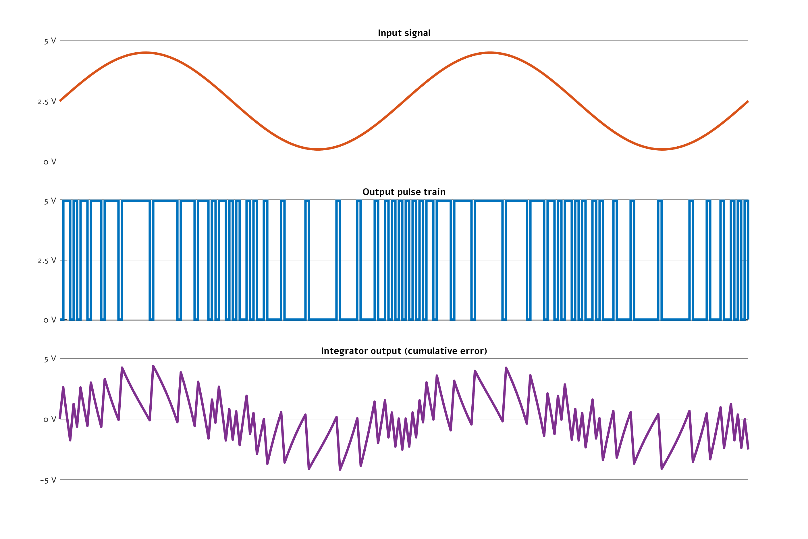
Although this may seem like a fairly unhinged approach to making precise signal measurements, the 1-bit stream produced by the comparator can be then digitally processed to compute the duty cycle of the seemingly-chaotic high-frequency pulses — and thus infer the analog input value. Best of all, because there are comparatively few potential sources of analog errors, the linearity is superb. On the flip side, to achieve reasonable precision, the clock used to operate the ADC must be much faster than the desired analog sample rate.
The same “delta-sigma” moniker is also used to refer to a subclass of oversampling interpolating DACs that employ similar pulse modulation, as discussed earlier. That said, they’re not nearly as clever: the bulk of the pulse modulation happens in the digital realm, with no cute analog feedback loops to speak of.
👉 For more articles on electronics, click here.
I write well-researched, original articles about geek culture, electronic circuit design, and more. If you like the content, please subscribe. It’s increasingly difficult to stay in touch with readers via social media; my typical post on X is shown to less than 5% of my followers and gets a ~0.2% clickthrough rate.
The 1-bit pulse train thing is also a common way to build an amplifier. Instead of trying to amplify a delicate analog signal, people just feed the output of a sigma-delta DAC into some beefy MOSFETs and perhaps a low pass filter if the're feeling generous. The output has next to no distortion, because the power transistor never sees the analog waveform.
As a bonus, because the transistor is always full on or fully off, the efficiency approaches 100%, and only very minimal cooling is needed.
A similar trick is used for radio transmitters: Most transmitters that work by feeding a square wave at around into big MOSFETs driving a band-pass filter. That's enough for FM, but for AM, they feed power though a another MOSFET driven by a PDM signal and a low-pass filter.
This gives an exceptionally clean output, again at near 100% efficiency, which is important when putting out kilowatts or megawatts.
ADC/DACs are still relevant, but I'd say digital is eating the world! Your two analog examples are actually great use-cases for all digital signal chains.
For image capture, you get much better dynamic range and lower noise if you capture pixels as single bits integrated over time. So, for example, you charge up a pixel array and then check all the pixels periodically to see which have flipped. Brightly illuminated pixels flip quickly. You get to pick how long you want to wait. At the limit, you can have pixels that are single photon detectors/counters (these actually exist today, just too low res for cameras... for now). Light itself is inherently digital, better to process it in its native domain! :)
The most efficient and lowest distortion way to drive a speaker is similarly digital. You basically send a series of bits at a much, much higher frequency than the highest audio frequency thought the entire amp chain and then let the inductance of the speaker coil integrate all the bits into the movement of the cone. Because the amps are driven rail to rail with very well defined edge transitions, they spend as little time as possible in their noisy and power hungry non-linear region. Here is also no noise to get amplified- you just get out much stronger versions of the exact same bits you put in.