
Clocks in digital circuits
How do electronics keep track of time - from RC oscillators, to quartz crystals, to phase-locked loops.
Clock signals are the backbone of modern computing. Their rising or falling edges synchronize CPU state transitions, assist in shifting bits in and out on data buses, and set the pace of countless other digital housekeeping tasks.
Operating complex systems off a single clock is usually impractical: a computer mouse doesn’t need to run at the same speed as the CPU. A typical PC relies on dozens of timing signals, ranging from kilohertz to gigahertz, some of which aren’t synchronized to a common reference clock. The clocks originate in different parts of the system and are dynamically scaled for a variety of reasons: to conserve energy, to maintain safe chipset temperatures, or to support different data transmission rates.
In this article, we’ll have a look at how digital clock signals are generated, how they are divided and multiplied, and where they ultimately end up. The write-up assumes some familiarity with concepts such as inductors and op-amps; if you need a quick refresher, start here and here.
Clock sources: RC oscillators
The most common digital clock source is an RC oscillator: a simple device constructed out of a capacitor, a resistor that sets the capacitor’s charge and discharge rate, and a negative feedback loop that flips the charging voltage back and forth. Because all these components can be easily constructed on the die of an integrated circuit, RC oscillators are commonly found inside microcontrollers and CPUs.
But how do you make a circuit oscillate? A naïve take is that we could just invert an input signal (e.g., 0 V → 5 V, 5 V → 0 V) and then loop the output back onto the input. This way, the device should be stuck in a perpetual cycle of transitions between the two voltages. To control the frequency, we can add a delay mechanism, such as a capacitor charged via a resistor, in that loopback path.
It would appear that the simplest way to build this circuit is to take a single NOT logic gate, which can be found in “glue logic” chips such as 74HC04:
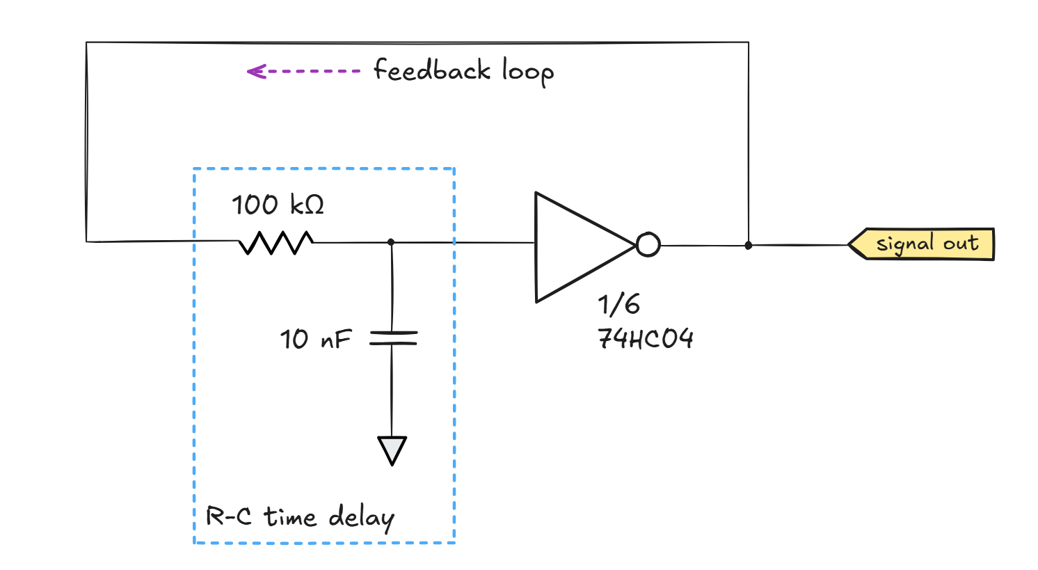
In practice, however, the circuit will not function correctly. Most of the time, the underlying analog nature of digital circuitry will rear its ugly head, and the circuit will reach a very non-digital equilibrium somewhere around Vcap = Vout = Vdd/2 — essentially, a halfway position between “on” and “off”. At that equilibrium point, any slight increase in Vout pulls the input voltage higher, which in turns causes the output to move back toward the midpoint; the inverse happens if Vout drops. This linear negative feedback loop prevents oscillation.
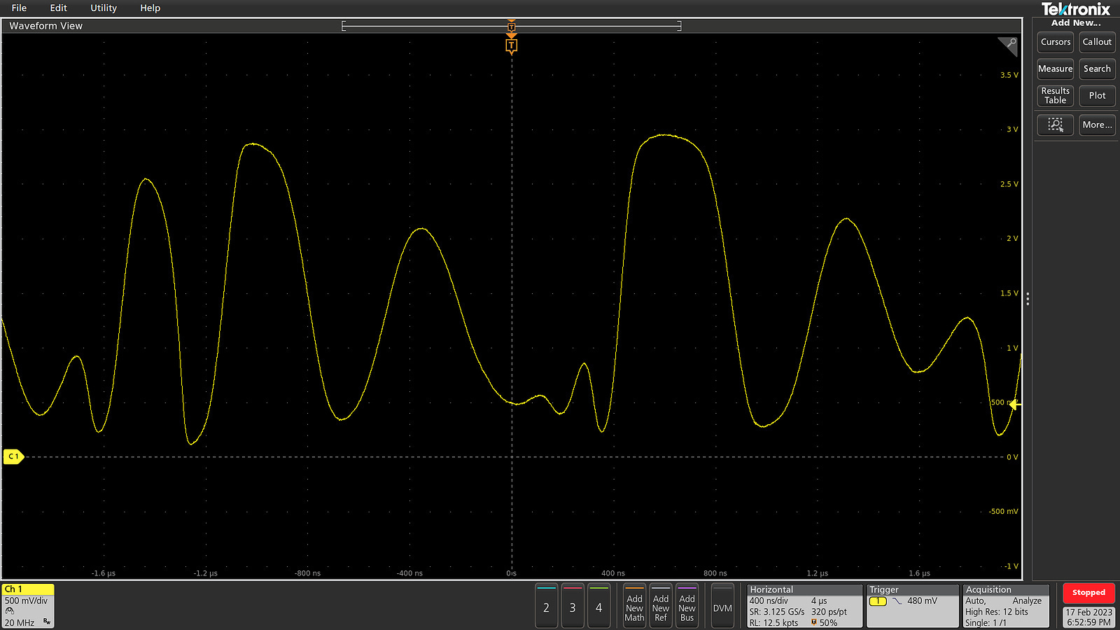
With some nudging (e.g., a sufficiently noisy power source), the high-gain analog amplifier that masquerades as the NOT gate might be knocked out of the equilibrium with enough force for some measurable oscillation to happen. But if so, the result will be some sort of a chaotic mess:
A “linear” circuit like this could be fixed by removing the RC delay section and replacing it with a more elaborate circuit that ensures a roughly half-wavelength phase shift between the output signal and the input at a single chosen sine-wave frequency. At other frequencies, excursions from Vdd/2 will continue to interfere destructively, but at the design frequency, the input will appear flipped around (shifted 180°) from the current output, producing a positive feedback loop that pushes the voltage out of equilibrium, not back into it.
We’ll circle back to this phase-shift concept in a while, but oftentimes, it’s easier to build an oscillator by getting rid of the stable equilibrium for the circuit to settle into. A particularly elegant circuit is the following rail-to-rail op-amp design:
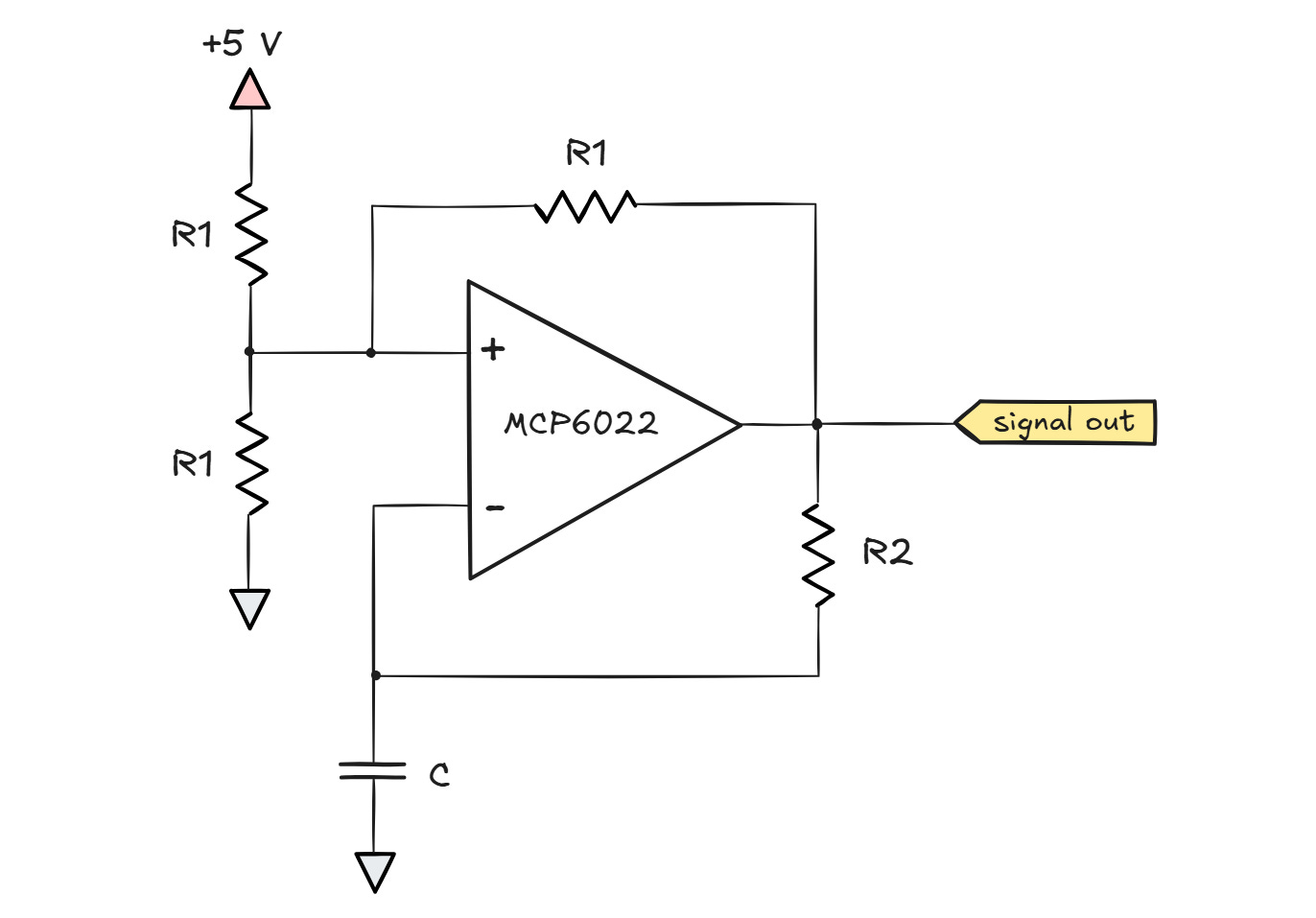
First, let’s have a look at the non-inverting input: with three identical R1 resistors, the voltage on this leg is a simple three-way average of 0 V, the supply voltage (Vdd = 5 V), and whatever level the output of the op-amp happens to be at a given time. In other words, Vin+ can only range from 1/3 Vdd (if Vout = 0 V) to 2/3 Vdd (if Vout = Vdd).
Now, let’s examine the inverting leg. Assume the capacitor is initially discharged, so Vin- = 0 V. Because Vin+ >> Vin-, the output of the op-amp jumps toward the positive rail and the capacitor begins to charge. The situation continues until Vin- reaches Vin+, which at that point sits at 2/3 Vdd.
The moment the input voltages meet, the output voltage of the op-amp will decrease — perhaps not all the way to down, but it will drop a notch. This instantly pulls the Vin+ leg lower because the output voltage is responsible for one-third of the signal present on Vin+. At that point, Vin- >> Vin+ — in effect, we enter a downward spiral that causes Vout to plunge all the way down. The capacitor now begins to discharge — and will continue to do so for a while, because it now needs to go down to the new Vin+ voltage — 1/3 Vdd — before another flip can occur.
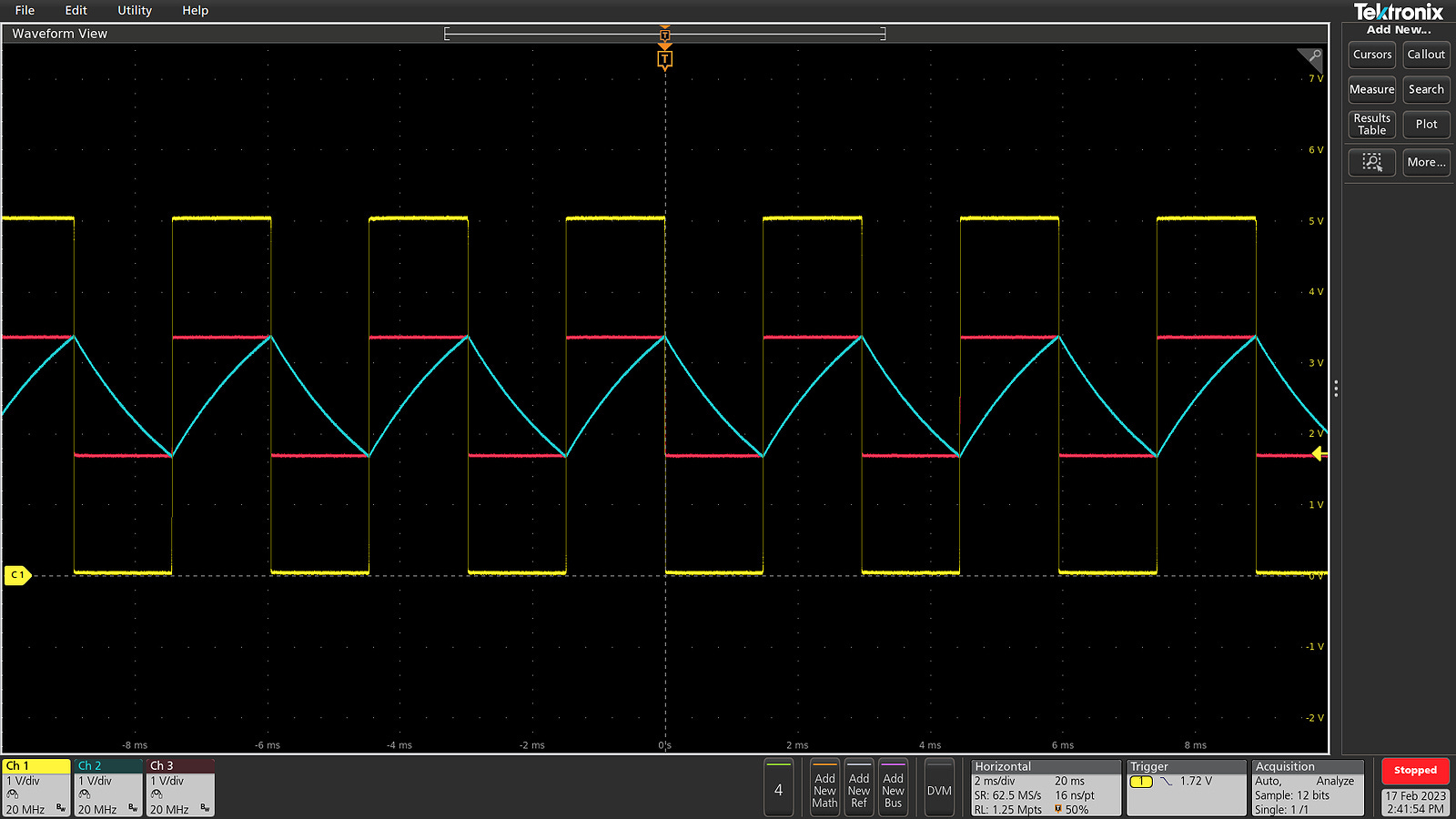
In effect, we have a binary circuit with hysteresis: the transition from “0” to “1” takes place at a much higher voltage than from “1” to “0”. With no stable equilibrium and two distant transition points, the arrangement functions as a good oscillator. The following oscilloscope plot shows the oscillator’s output voltage (yellow), along with the op-amp’s inputs: Vin- (blue) and Vin+ (pink).
A similar kind of memory / hysteresis can be built into CMOS digital logic using a simple two-transistor arrangement. Logic gates with this property are described as having “Schmitt trigger” inputs. One example is the 74HC14 Schmitt trigger inverter, which can be used to build a working version of the ill-fated NOT gate oscillator discussed earlier on:
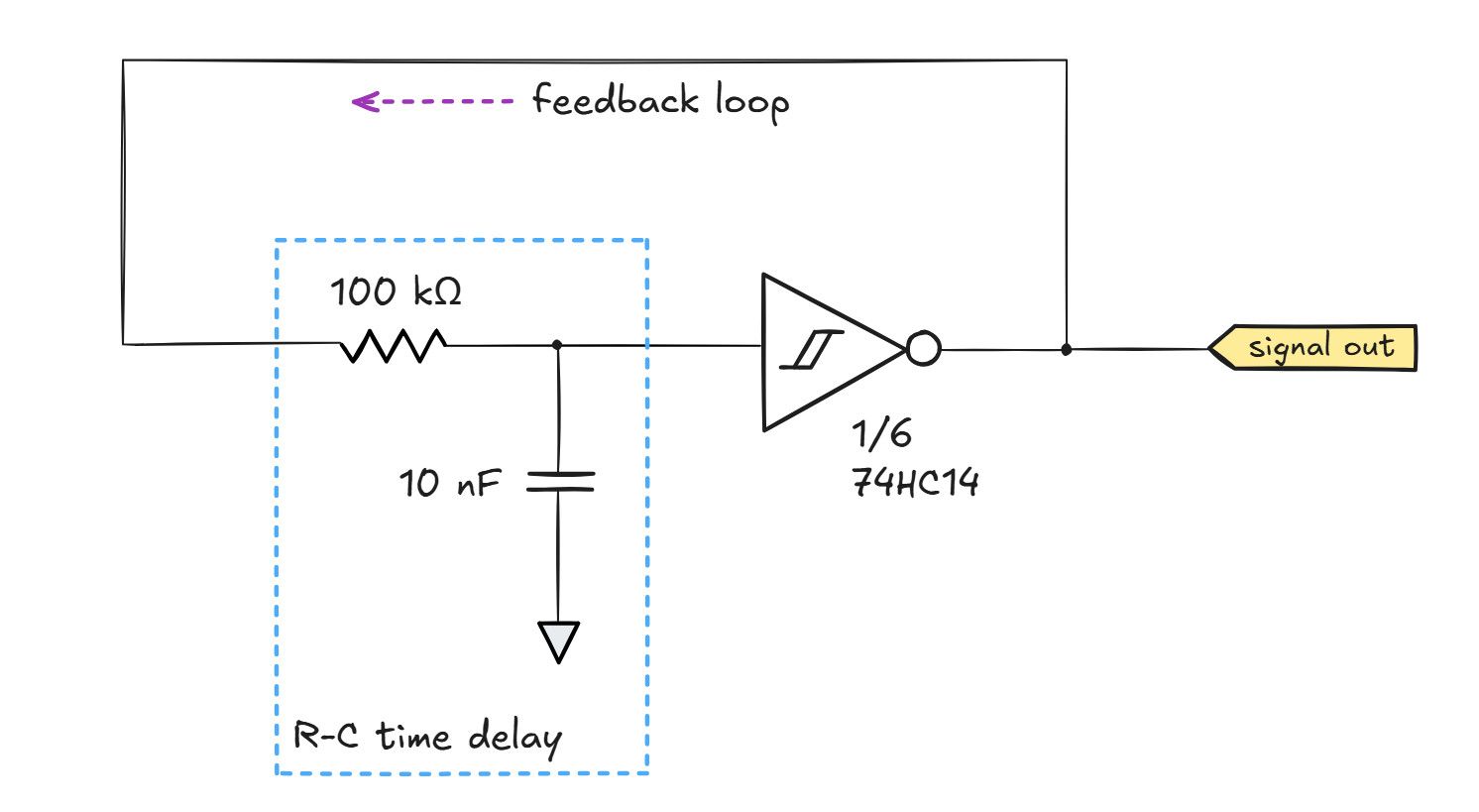
The oscillation period of these circuits is dictated by how long it takes to move the voltage across the capacitor back and forth between the two transition voltages.
Clock sources: piezoelectric materials
Although RC oscillators are easy to make, they are not particularly accurate: standalone capacitors are typically made with an accuracy of 10% or worse, and are profoundly affected by temperature and aging. With some care, accuracy down to 2-5% can be achieved; this is good enough for general computation, but it gets in the way of precise timekeeping, and may interfere with some clock-sensitive protocols, such as USB.
The quest for better accuracy brings us to a peculiar electromechanical device: a laser-trimmed piece of piezoelectric material — often quartz — that produces a coherent electrostatic field on its surface when squeezed. Piezoelectric materials are used to generate sparks in some push-button igniters, but the effect is symmetric: the application of an electrostatic field can cause the material to contract and then elastically return to the original dimensions once the voltage is removed. This leads to a couple of other niche applications, including ultra-miniature but wimpy motors used in camera lenses, along with high-frequency buzzers used in smoke alarms and ultrasonic range sensors.
Piezoelectric crystals also make good resonators. Much like a kids’ swing, if you send pulses that contract the crystal at its natural resonant frequency, it’s easy to get it going and reach a considerable amplitude of motion without applying a whole lot of force. Conversely, if you time your pushes wrong, the swing won’t go very far, and you might get your teeth knocked out.
The following video illustrates the moment of hitting the resonant frequency of a quartz crystal. At that point, the crystal’s AC impedance is at its lowest — that is, a given driving voltage (yellow) achieves the maximum current swing (blue):
At that exact point, there’s also little phase difference between the driving voltage and the resulting current measured across the device.
Curiously, the behavior of the crystal around its resonant frequency is asymmetric. Delivering pulses a bit too slow causes a more gradual reduction of amplitude than delivering them slightly too fast. In the latter case, we quickly hit what’s known as anti-resonance: a point where the impedance skyrockets and there’s very little current flowing through the device. The swing analogy helps understand what’s going on: if you push the swing a tiny bit too late (i.e., as it starts moving away from you), you’re not going to transfer energy as efficiently but it’s not a big deal. But if you push it too early — while it’s moving toward you — you’re actually braking it. Do it a couple of times and the swinging will stop.
In addition to changes in impedance, we can also observe shifts in phase between the applied voltage and the resulting current. Most of the time, when the crystal is not oscillating, it’s electrically just a capacitor: two metal plates and some non-conductive layer sandwiched in between. It follows that across most of the frequency rance, there’s a capacitor-like -90° phase shift where the current peaks are one-fourth of a cycle ahead of the peaks in the applied AC voltage.
That said, between the resonant and anti-resonant frequency — in the “braking” region — the relationship is briefly reversed. In effect, for a moment, the crystal behaves a bit like an inductor, even though it isn’t one in any conventional sense:

Perhaps the most logical way to build a crystal-driven oscillator would be to zero in on the region of minimum impedance (the dip on the top plot, marked with the dashed line). Yet, the most common architecture used in digital circuits — the Pierce oscillator — works differently. It zeroes in on the region where the crystal exhibits inductor-like current lag. The target phase shift is typically in the vicinity of 90°, somewhere on the upward slope to the right of the dashed line.
The Pierce oscillator isn’t explained clearly on Wikipedia or on any other webpage I know of, but the basic architecture is as follows:
We can start with the inverter: it does just what the name implies. For steady sine waves, inverting the signal is the same as creating a 180° phase shift between the input and output voltages. For simplicity, the circuit usually isn’t constructed with a well-behaved op-amp. Instead, it uses a basic, high-gain NOT gate. This also explains the resistor on top (Rlin): it’s simply a kludge to achieve semi-reasonable linearity when using the wrong component for the job. The resistor provides a degree of negative feedback, adding the inverted signal to the input and thus reducing the NOT gate’s gain.
The next portion of the circuit is the series Rser resistor connected to a shunt capacitor (C1). Most simply, this forms an RC lowpass filter. The components are chosen so that the circuit operates well above the lowpass cutoff frequency, thus adding close to 90° signal phase shift between the output of the inverter and the right terminal of the crystal.
Finally, when the crystal acts as an inductor and charges a shunt capacitance C2, the components form an LC lowpass filter capable of adding another shift of about 90°. The key point is that the second filter can work only if the frequency of the signal falls within the narrow inductor-like region of the crystal; otherwise, this combination of components just forms a useless two-capacitor section and the circuit doesn’t oscillate.
I should note that this explanation isn’t quite right: the RC filter and the LC filter aren’t isolated from each other, so so there are some parasitic interactions between these stages; for an analysis of a similar scenario, you can review this article. That said, as long as the impedance of the second stage is comparable to or higher than the first stage, the simplified model is pretty accurate.
The main reason we use this architecture is that it requires the minimum number of external components: the inverter and the resistors can be placed on the MCU die, so in most cases, you only need two small, picofarad-range capacitors in addition to the crystal itself.
Because Pierce oscillators operate slightly above the crystal’s true (“series”) resonant frequency, some attention must be paid when shopping for components. Most crystals are specified for use with Pierce oscillators, but some may be characterized at their series frequency — and will run a tiny bit fast when connected to an MCU. The difference usually hovers around 100-300 ppm, but this is nothing to sneeze at if you consider that the crystal’s usual accuracy is around 20 ppm.
Crystal oscillators can’t be easily manufactured on a silicon die, so they almost always come as discrete components, set apart by their shiny metal cans. It’s most common to encounter crystals between 1 and 40 MHz, although a peculiar value of 32.768 kHz is also a common sight (more about that soon).
Clock sources: MEMS
In recent years, microelectromechanical (MEMS) oscillators emerged as an alternative to quartz crystals in some applications. Similarly to quartz, they rely on a precision-tuned mechanical oscillator, although the vibrations are induced in a different way.
The devices don’t offer any significant advantages or disadvantages compared to quartz, except for making it easier to put active control circuitry on the same die as the resonant structure itself. This saves a tiny bit of PCB space and allows internal adjustments to output frequency (see below), so MEMS clock sources tend to crop up in high-density applications such as smartphones or smart watches.
Clock division
Modern computers operate at gigahertz frequencies, but such clock speeds are reserved only for a handful of system components, and only during peak demand. Gigahertz signals pose significant design challenges for larger circuits; plus, there’s no conceivable need for an audio chipset or a fan controller to run nearly that fast.
For this reason, it’s common for clock signals in digital circuits to be divided (“prescaled”) for specific subsystems. The simplest and oldest way of doing this is to clobber together a handful of logic gates and build a binary counter (or use an existing counter chip, such as 74HC393). This allows the signal to be divided by any power of two:
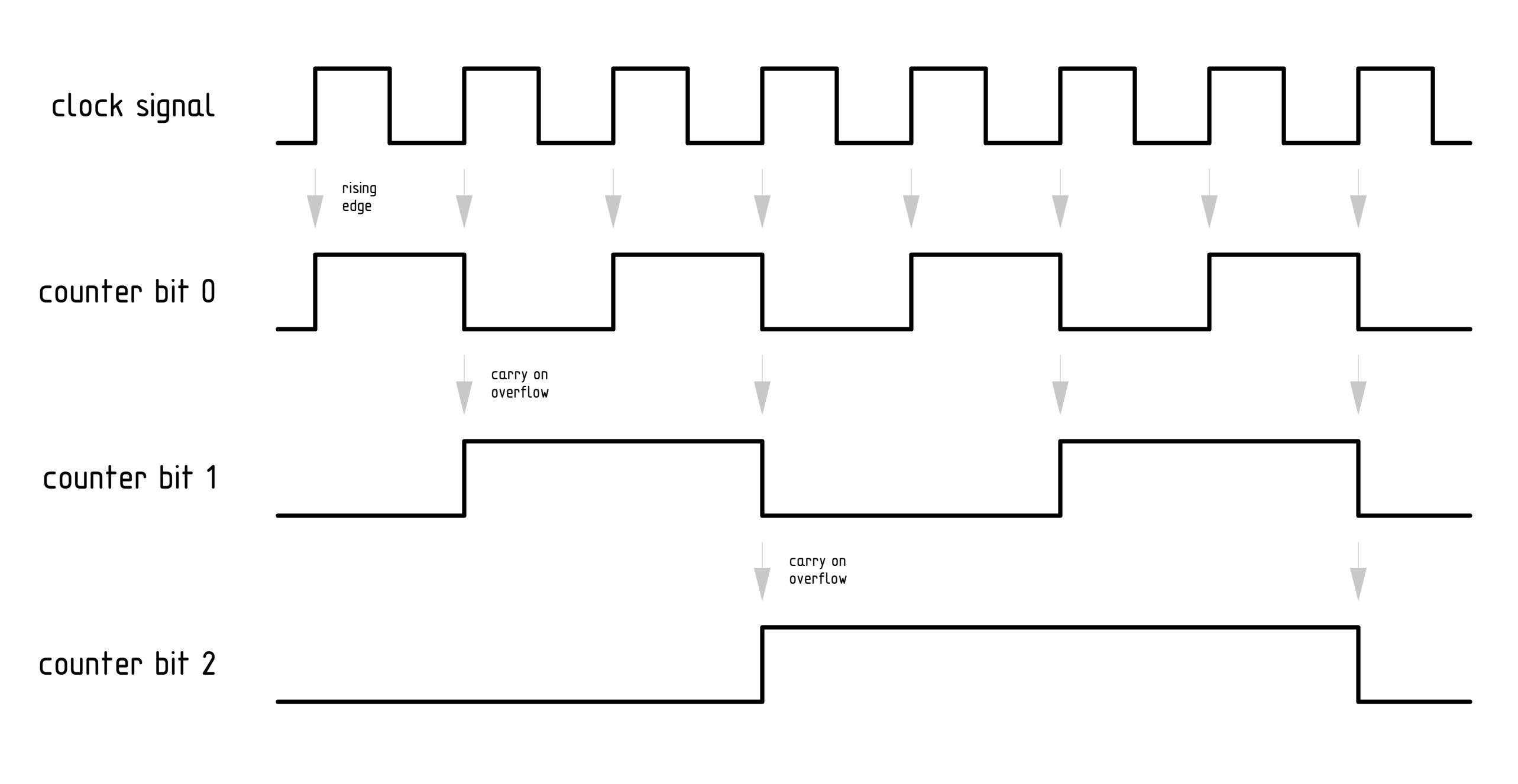
The approach brings us back to the curious case of the 32.768 kHz oscillator: it originated in the era of digital watches, where its signal could be divided using a binary counter to get one second ticks (32768 / 215 = 1). Today, thanks to higher transistor densities and better power efficiency, arbitrary divisions can be accomplished with countdown circuits that start from a preprogrammed value and then reload the register after reaching zero. That said, the 32.768 kHz clock still crops up all over the place, a darling of circuit designers and software engineers alike.
Clock multiplication
Note: this section is also available as a standalone article here.
Clock division is not a cure-all; for one, it’s pretty hard to make traditional crystal oscillators with resonant frequencies above around 60 MHz. Although some shenanigans with harmonics can be pulled off, it follows that if a modern CPU needs to run off a stable clock while attaining gigahertz speeds, we might need to employ some clever trickery.
Compared to clock division, multiplication is a bit more involved. The journey starts with a phase error detector. There are several ways to construct this circuit; about the simplest architecture is the following:
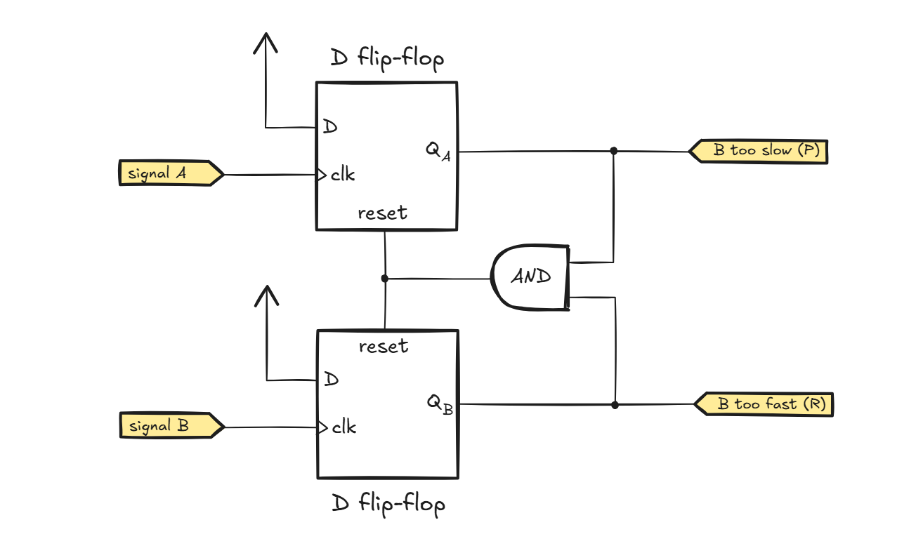
The purpose of the detector is to compare clock signal B to a reference clock provided on input A. If the positive edge on input A arrives before a positive edge on input B, the output of the upper latch (QA) goes high before the output of the bottom latch (QB), signaling that clock B is running too slow. Conversely, if the edge on B arrives before the edge on A, the circuit generates a complementary output indicating that B is running too fast. After a while – once both clocks are positive – the latches are reset.
The following plot shows the behavior of the circuit in the presence of two different frequencies of signal B:
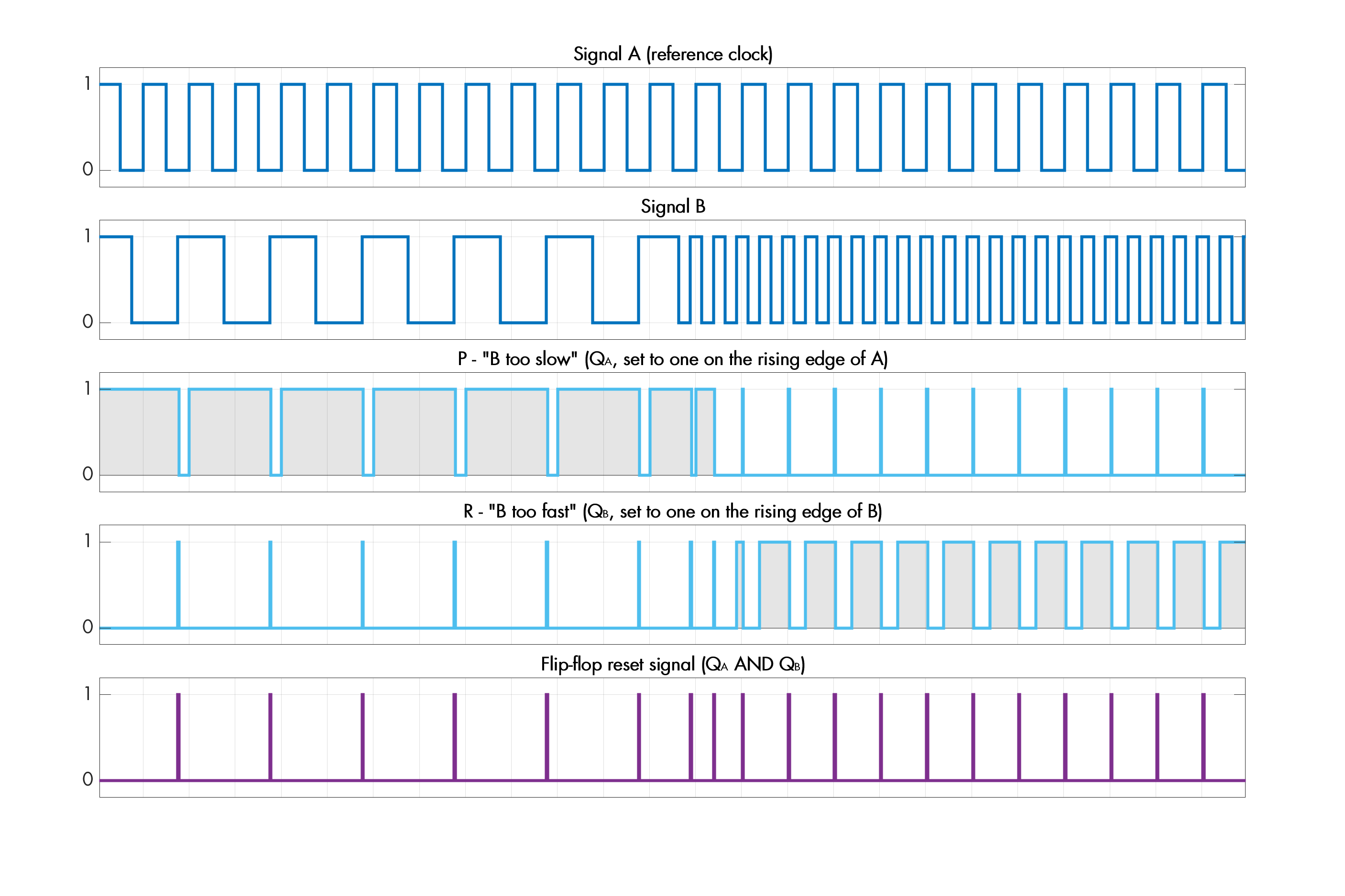
In effect, the detector generates longer pulses on the output labeled P if the analyzed clock signal is lagging behind the reference; and longer pulses on the other output (R) if the signal is rushing ahead.
The detector is the fundamental building block of a circuit known as a phase-locked loop (PLL). Despite the name, the main forte of phase-locked loops is matching the device’s output frequency to an input signal of some sort:
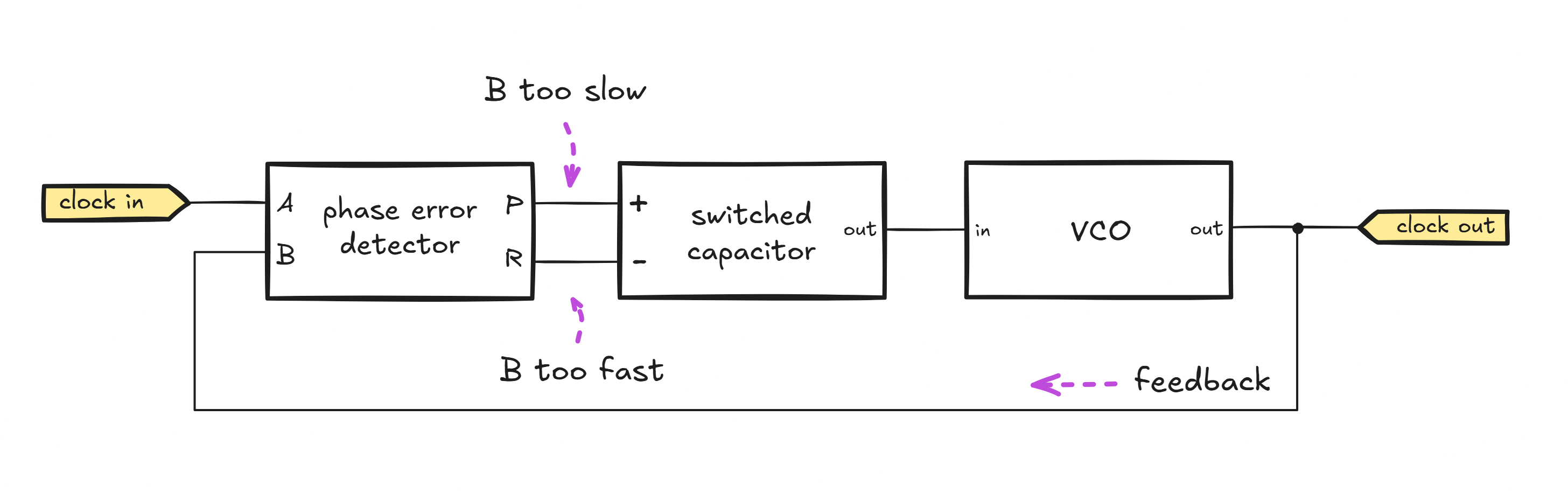
The output stage of the PLL is a voltage-controlled oscillator (VCO), which generates a square wave with a frequency proportional to the supplied input signal.
The voltage for the VCO is selected by a simple switched capacitor section in the middle; the section has two digital inputs, marked “+” and “-”. Supplying a digital signal on the “+” input turns on a transistor that gradually charges the output capacitor to a higher voltage, thus increasing the frequency of the VCO. Supplying a signal on the “-” leg discharges the capacitor and achieves the opposite effect.
The final element of the circuit is the phase error detector; it compares the input clock to the looped-back output from the VCO. The detector outputs long pulses on the P output if the VCO frequency is lower than the external clock, or on the R output if the VCO is running too fast. In doing so, it adjusts the capacitor voltage and nudges the VCO to match the frequency and phase of the input waveform.
This fundamental circuit has a number of uses in communications; PLLs are useful for radio demodulation and clock reconstruction for digital data streams. Nevertheless, the architecture doesn’t seem to be doing the one thing we’re after: it’s not a clock multiplier.
To address that issue, we just need a small tweak:
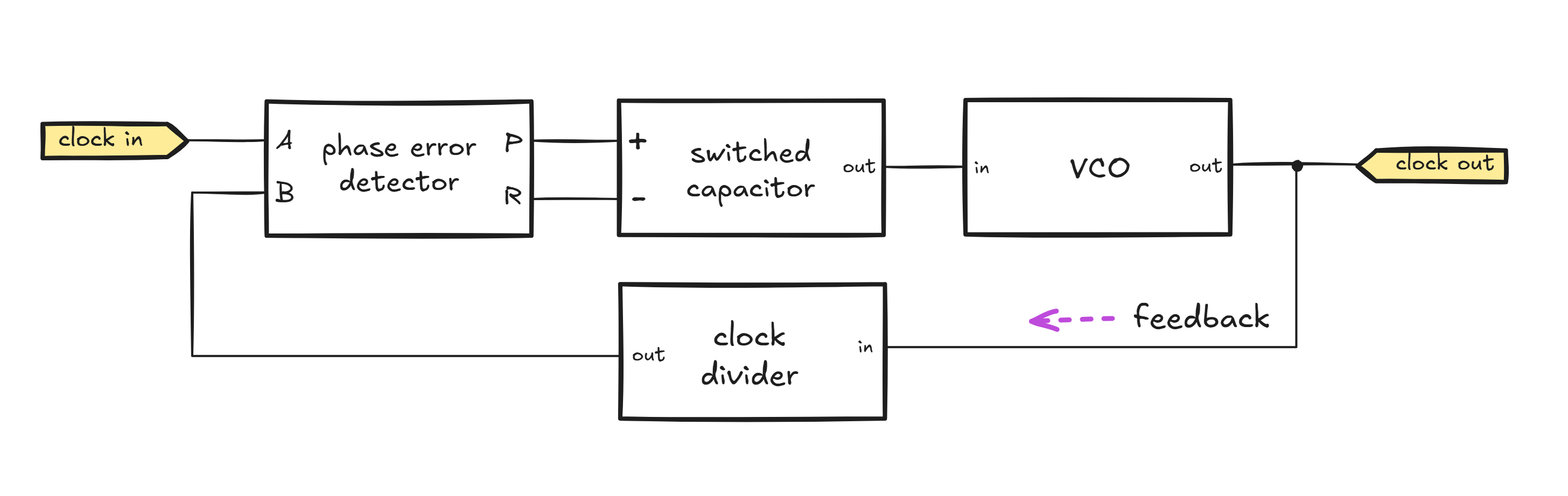
We added a frequency divider in the feedback loop. With this modification, the phase error detector circuit will nudge the VCO until the divided output signal matches the input clock. If the frequency of the looped-back signal is halved in relation to the VCO output, the oscillator will need to run at twice the frequency of the input clock for the PLL to achieve lock. This gives us a precise and versatile frequency doubler — and of course, other multiplication ratios can be realized too.
System-wide clock architectures
In the classical PC architecture, the processor’s job is to handle computation; most other tasks — from storing data, to drawing graphics on the screen, to handling I/O ports — are delegated to other chips. Although there is a trend toward greater integration, in such environments, you can usually find a mid-speed clock, perhaps in the vicinity of 100 MHz, distributed to various portions of the motherboard. This clock is then divided and multiplied to suit specific needs; for example, the CPU has its own multiplier, a matter of great interest to overclocking enthusiasts. Of course, there is also a fair number of embedded controllers and external peripherals that operate with their own free-running clocks, talking to the main system via slower, explicitly-clocked serial I/O.
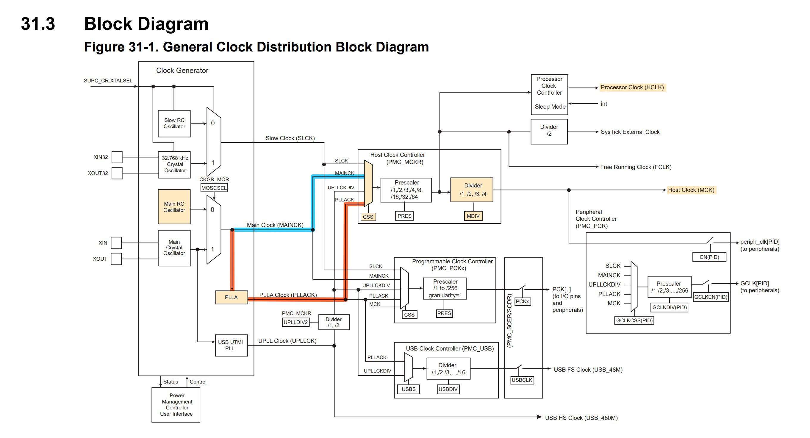
In microcontroller and system-on-a-chip environments, the level of integration is typically much greater. A typical 32-bit MCU will have an internal RC clock source, along with a Pierce oscillator that can be hooked up to an external crystal if desired. A number number of internal PLLs and clock dividers will be available to generate higher frequencies for the CPU core, and lower frequencies for flash memory or for USB:
In embedded systems, MCU clock is seldom distributed to external components; host-generated clock signals might be provided as a part of buses such as SPI or I2C, but they are supplied intermittently, so devices that need to do anything in between the transmissions would need a clock of their own. As a practical example, an SPI DRAM chip such as APS1604M-3SQR will have an internal RC oscillator to handle periodic memory refresh. The same goes for many ADCs, display modules, and so on.
👉 For further articles about electronics, click here. In particular, you might enjoy:


I write well-researched, original articles about geek culture, electronic circuit design, algorithms, and more. If you like the content, please subscribe.
Of course, the marketplace of clock sources is a bit of a rabbit hole on its own.
In addition to standard xtals, there are temperature-compensated or temperature-controlled variants (TXCO and OCXO), the latter reaching parts-per-billion accuracy (but also costing a lot). Then, there are ceramic resonators, made from the same material as piezoelectric transducers; this is cheaper than quartz and less bad than RC circuits - good enough for applications such as USB or Ethernet. Finally, there are integrated modules that might contain an amplifier and a programmable divider / PLL.
Thanks! What I still don’t quite understand is where I would “apply” voltage in the inverter based circuit. I guess an inverter is a mosfet or two? And that comes with a power source, and so the output of the inverter starts at a (presumable low) voltage and then tries to invert it, and then it “gets going”.
Do they have a polarity? An optimal voltage range (maybe that comes down to the inverter/amp circuitry)? I recall their data sheets being a bit thin but it’s been a while since I looked.
Maybe I need to put some things on a breadboard to get going.
My question is kinda like: if I have a couple volts somewhere (probably more like 100mV AC for a short period), and I wanted to make some oscillations at a known frequency how would I go about it?