
Analog filters, part 2: let it ring
A continuation of the gentle intro to analog signal filtering. In today's episode: transfer functions, Q factors, and the Sallen-Key topology.
In an earlier article on analog signal filtering, we talked about basic RC filters. My thesis was simple: that despite the efforts of Wikipedia editors, the behavior of these devices can be understood and modeled without resorting to obtuse jargon or advanced math.
The main subject of that article was a rudimentary first-order RC lowpass filter, constructed the following way:
To readers with good intuition about capacitors, the qualitative analysis should be simple. At low frequencies, the cap has a high impedance, so sine waveforms pass through unhindered. At high frequencies, the capacitor behaves like a low-impedance shunt to the ground — and the amplitude of the waveform is greatly reduced.
To make this a bit less hand-wavy, we also derived the formula for a midpoint frequency where the resistance of the resistor matches the reactance of the capacitor:
We established that at this particular frequency, the output sine wave of a basic first-order RC filter is attenuated to √½ (~70%) of the input amplitude. Last but not least, we plotted the filter’s behavior across a range of frequencies on a log scale:

Toward the end of the article, I noted two practical problems with this design: the attenuation slope is not particularly steep, and there is a pronounced, rolling transition between the passband and stopband region. This is a far cry from the “brick wall” response that some users might be aiming for.
Today, let’s have a look at how to solve these issues in real life.
Bending the slope
If we have a way to attenuate high frequencies while passing low-frequency signals largely unchanged, the most obvious way to beef it up is to use the filter twice:

Logically, the effects should stack. If you have a knob that reduces volume by 50%, and you put another 50% knob after it, you’d expect the signal to be reduced to 25%; similarly, if the attenuation offered by a single-stage filter is x at some chosen frequency, then with two stages, it should be x².
That said, if we build the circuit, we might find out that it’s not behaving quite as expected. The mathematical model of this circuit is somewhat tedious to develop, so we can start with a qualitative evaluation. Let’s consider the worst case where the values of R1-C1 and R2-C2 are chosen to have the same fc, but the second stage has much lower impedance. For example, we could choose 10 kΩ + 100 nF for the first stage, and then 100 Ω + 10 µF for the second.
Because the stages are not separated, this means that C2 is free to source current directly from the input via the R1 + R2 path — and in this case, because R1 ≫ R2, the resistance of this path is ≈ R1. This essentially forms an unwanted R1-C2 filter with a different frequency response curve and a lower fc.
Meanwhile, the first capacitor (C1) can source current through either of the parallel resistances — but again, because R1 ≫ R2 and because the impedance of C2 is much smaller, it can preferentially charge via that path. This forms a parasitic R2-C1 filter, and the result is this beautiful mess:

You can distinctly see the first kink at the center frequency of the R1-C2 filter (fc ≈ 1.6 Hz); and then another kink at the center frequency of the second filter formed by R2-C1 (fc ≈ 16 kHz). This is pretty far from the design frequency of fc ≈ 160 Hz.
Next, let’s try to build a better model of this circuit. The following subsections are a bit math-heavy, so you can skip ahead — but the text offers interesting insights and should be a lot more accessible than most of what you can find on the internet.
Modeling a second-order RC filter
To develop a more precise understanding of the circuit, let’s start by looking at the three-way node on the right side of the schematic (B):

It’s a basic concept in circuit analysis that the momentary currents flowing into and out of any point must net out to zero: electrons generally can’t go sideways. For node B, assuming no substantial output load, the current flowing in through R2 must be equal to the current flowing out via C2 (or vice versa). This fairly obvious rule is known as Kirchhoff’s current law (KCL).
Notionally, peak sine-wave currents through a component are easy to calculate if we know the component’s impedance (Z = V/I) and the amplitude of the applied voltage signal. The problem is that in this setup — a pair of parallel components — the currents are not in phase. The current through a resistor is always in sync with the applied voltage; the current through a capacitor is one-fourth of a cycle (90°) out of whack with the applied sinusoid. This means that if we calculate the peaks, they don’t need to obey KCL, because they don’t occur at the same time!
Sinusoids that are 180° apart are an easy case: the waveforms just interfere destructively, so addition becomes subtraction. But the case of 90° is trickier; in the earlier article, we showed that it can be solved with trigonometry. We could take that route, but we’d be doing a ton of spurious calculations just to recalculate phases and amplitudes after every operation.
It’s better to use another trick outlined in that article: we’ve shown that the Cartesian coordinate system can be used to model the interaction of phase-shifted sines, because the rules for adding 0° and 90° sinusoids happen to be the same as the rules for calculating diagonals in the (x, y) plane. This allows us to keep track of the 0° component and the 90° component separately for the bulk of the analysis. And instead of two separate coordinates to describe resistive and reactive effects, we could be using the complex-number representation outlined a bit later in the linked post.
Don’t close the tab just yet! Complex numbers sound… complex, but this is actually the simpler route. It’s a game of cat-herding: we have a “real” part of the equation that represents sine wave signals with a 0° shift, plus an “imaginary” part that represents sinusoids shifted by 90°. The imaginary part is multiplied by a magic-bean symbol (the earlier article used 🐱 — but more conventionally, j). The symbol is used to keep the dimensions at an arm’s length, so it’s essentially just an expedient way of working with two orthogonal values at once.
Again, in the equations for node currents, we’d be keeping the effects of resistance in the real domain, but multiplying the effects of capacitors by j. When we’re done with all the algebra, we can split out the real and imaginary parts by gathering the terms with and without j, essentially going back to a 2D representation that can be worked on with ease.
To calculate currents, we’d normally be leaning on the formula for reactance — i.e., we’d be sooner or later calculating j·XC (and j·XL if we had any inductors in sight). This brings us to another time-saving trick: we can combine j with the repetitive 2πf part in the equations for reactance, and label that combined 2πfj expression as “s”. This lets us replace reactances directly with component values (L or C) while keeping visual clutter in check:
This is nice: we usually want to express circuit properties in terms of component values, so we now have fewer substitutions to make down the line.
Anyway, back to the circuit:
At this point, we have everything to write the equation that expresses the balance of currents at point B in the circuit in function of component values and node voltages:
The capacitor is connected between point B (Vout) and 0 V (ground), so the applied voltage is always Vout; the current is a function of Vout and the component’s reactance, which we replaced with 1 / sC2. Again, keep in mind that s incorporates j, so this also puts the capacitor current in the phase-shifted domain of imaginary numbers and prevents it from getting commingled with resistor currents.
As for the resistor, the voltage across its terminals is the difference between points A and B; the voltage at A (VA) is a new variable, while the voltage at B is equal to Vout. We don’t know Vout, and it’s actually something we’ll be solving for — but not just yet.
I won’t be boring you with grueling but basic algebra, so let’s cut to the chase. If we solve the aforementioned three-equation system for the voltage at node A, we get:
We arrived at this result by writing the equations for the currents flowing through node B; now, let’s repeat the analysis for node A. Here, we have three current paths: R1, R2, and C1 — and once again, we know the currents must balance out:
Solving this system of equations for Vout nets us:
Now, we plug the earlier equation for VA into this equation; after a fair amount of tidying-up, we get:
The Vout/Vin version is known as the filter’s transfer function — i.e., an equation that describes relative signal gain and phase at a given sine signal frequency f (hidden as a part of the s expression) and for given component values.
Examination of the transfer function
The transfer function has a combination of real and imaginary terms in the denominator; this can be cleaned up, but the reorganized equation ends up looking pretty gnarly.
Because the numerator is just “1”, the simplest shortcut we can take is to switch to the reciprocal function, which describes complex attenuation instead of complex gain. Let’s call it Ca:
Substituting s = 2πf·i, and remembering that s² yields a real expression (-4π²f²), we can now easily collect the magic-bean-free terms and get an equation for the real part of Ca:
The rest ends up in the imaginary bin, which we’ll keep separate, but with the j multiplier removed because it’s no longer needed to separate terms:
In effect, we’re back to Cartesian coordinates representing phase-shifted sine signals. Once again, the real part represents what’s going on at the 0° shift, while the imaginary part stands for 90°. Just like the complex impedances we started with, these equations still describe Cartesian coordinates on a two-dimensional plane. For specific component values and a given sine frequency f, we get a single point corresponding to signal response of the circuit.
If we have a point in two dimensions, we can calculate the distance to that point from the center of the coordinate system. This represents the scalar magnitude of attenuation and is given by the Pythagorean theorem:
Let’s plot this calculated distance across a range of frequencies, along with the absolute values of the real and imaginary expressions, and next to phase shift calculated with atan2(Im(Ca), Re(Ca)):

This looks… kinda right, except it’s a log-scale mirror image of the earlier plot. This is because we’re plotting the inverse of the transfer function. The result isn’t signal amplitude, but the extent to which the signal is attenuated! To flip it around, we’d just need a small tweak:
Meanwhile, the correct formula for phase shift is -atan2(Im(Ca),Re(Ca)).
That said, let’s stick to the “mirror image” version for a bit longer. The equations for the real and imaginary portions hold some interesting insights.
A closer look at the singularity
One of the benefits of taking the complex number route is that we can observe a peculiar singularity in the Re(Ca) curve that doesn’t show up in the combined plot. The value momentarily drops to zero somewhere in the middle of the flattened, 45° corner of the overall response curve.
Let’s have another look at the Re(Ca) equation:
We can note that the expression boils down to 1 - f²·const: component values are not supposed to change in a given circuit, so f is the only variable.
We can trivially solve for f at which Re(Ca) becomes 0. The singularity happens when the frequency-dependent contribution overtakes the constant value. The solution for this crossover frequency is:
It might be interesting to ponder why this dip doesn’t show up on the summed impedance plot. The basic answer is that we’re plotting on a logarithmic scale: every grid tick corresponds to a 10x increase or a 10x decrease in the underlying value. This means that when one curve is underneath the other component by two grid ticks or more (i.e., its value is 100x+ lower), it has a negligible impact on the sum. Because of this, the effects of the Re(Ca) dip are masked, and the shape of the filter’s response curve is a mirror image of the “roofline” formed by the maximums of the dashed curves.
Looking at the visualization a bit more, we can tell that to the left of the singularity, the curve is essentially a flat y = 1. In this section, the 4π²f²·R1·R2·C1·C2 part is much smaller than one and has virtually no influence on the value. A bit past the dip, this f²-part of the expression becomes much larger, and we get a segment more or less described by y = f²·const.
Meanwhile, the Im(Ca) curve is just a 45° diagonal given by y = f·const. The constants in the two equations aren’t the same, but what I’m trying to highlight is that in all cases, f is the only variable. Again, the rest depends only on component values, which are fixed within the scope of a specific circuit.
If we don’t care about modeling the exact curvature of the Re(Ca) singularity, we can reduce the plot to three straight lines. Let’s do that, taking note of the three intersection points: A (green × yellow, corresponding to the first bend in the filter’s response curve), B (green × red, the location of the singularity), and C (yellow × red, second bend):
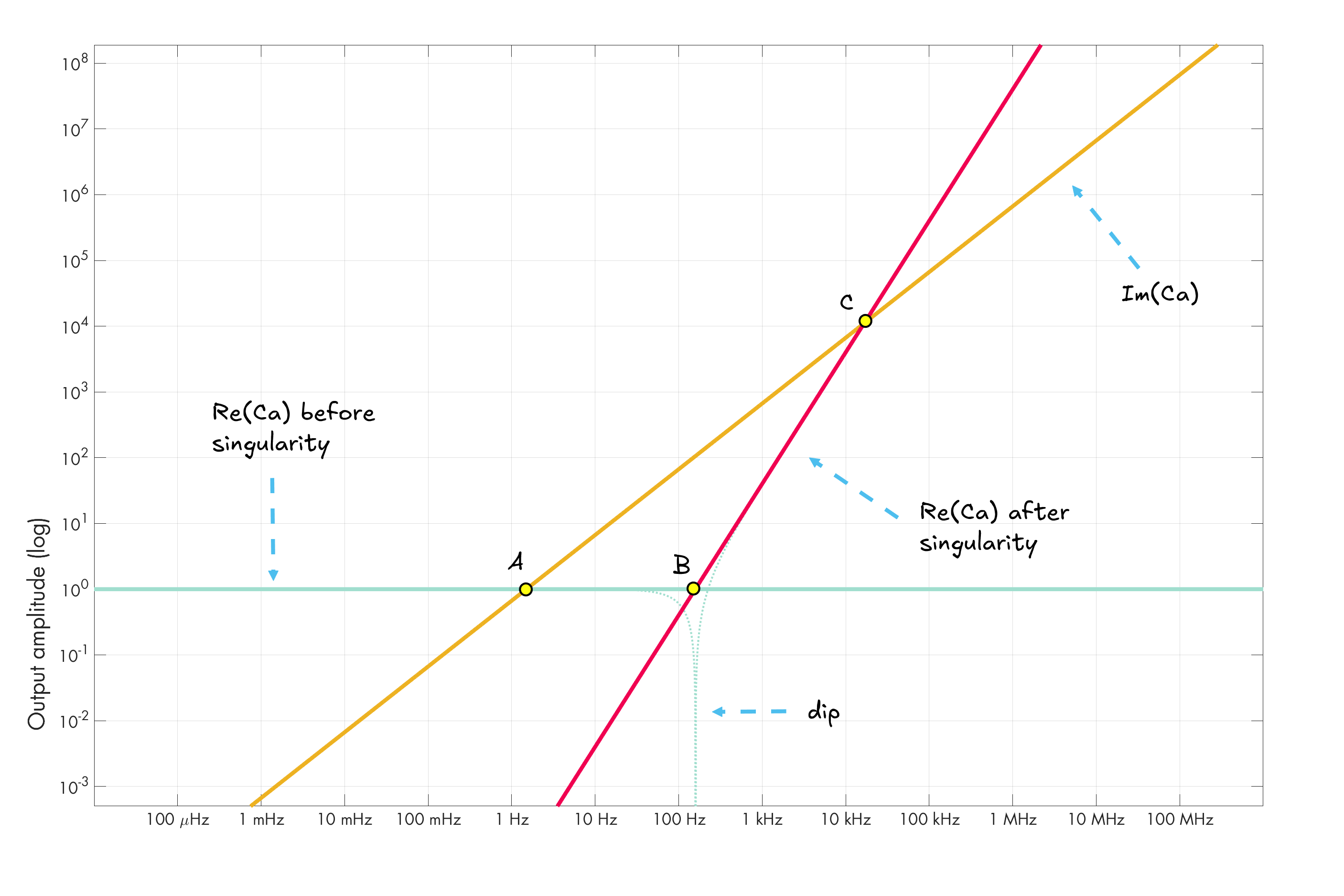
Next, let’s try to figure out the relationship between the yellow and the red line. We know their curvatures are described by y = f and y = f², along with some constant multipliers for each. If these multipliers were both equal to 1, the curves would be crossing the y = 1 line at f = 1.
Of course, they cross in different spots. We should note that log-plot distance units aren’t constant increments; instead, they express separation by orders of magnitude. To move either of these lines by one grid unit to the left, we’d need to multiply its parameter (f) by ten. This would move the crossing point from f = 1 to f = 0.1.
The above reasoning tells us that compared to the red line, the yellow line’s constant multiplier for f must be greater by some factor n equal to the log-plot distance between A and B at y = 1. We don’t need to find n right now. The goal is just to rewrite the two line equations in terms of some new, common constant z (which we also don’t need to solve for!), along with a multiplier n describing the horizontal distance between A and B:
Again, this puts point A (yellow line) at fA = z / n and point B (red line) at fB = z.
Since we have a pair of equations describing the two diagonal lines, we can also solve for the frequency at which they intersect (point C). This is simply:
So, point A is at fA = z / n, point B is at fB = z, and point C is at fC = z · n. This tells us that points A and C are log-scale equidistant from point B, which is also the location of the singularity.
As it turns out, the formula for the singularity frequency — f = 1 / (2πf√(R1·R2·C1·C2)) — gives us the midpoint of the filter’s “knee”, no matter how flattened it happens to be!
The Q factor
We can also use the same approach to find out the value of n. Again, this describes the horizontal log-scale span of the flattened section (well, one half of it).
As a reminder, we introduced n as a scaling factor defining the ratio of f-multiplying constants in the formulas for Re(Ca) and Im(Ca). So, we can just look at the equations and pluck out the f multipliers verbatim:
For the scenario we’ve been looking at (R1 = 10 kΩ, C1 = 100 nF, R2 = 100 Ω, C2 = 10 µF), n is a bit over 100. Because the flattened section has a downward 45° slope starting from point A, the horizontal distance from A to B is equal to the vertical rise in attenuation from the y = 1 line. For this passive filter, the lowest attainable value is n = 2, so we have 50% signal attenuation at the midpoint.
In practice, it’s more common to report the reciprocal value of n, which is known as the Q factor:
To restate the earlier point in these terms, the Q factor approaches 0.5 for an optimally-designed passive second-order RC filter, although in the instance we’ve analyzed, it’s less than 0.01.
As a parting observation, here’s what would happen if we divided Im(Ca) by some number to move the yellow line down, and then recalculated the filter’s response curve from the Pythagorean theorem:
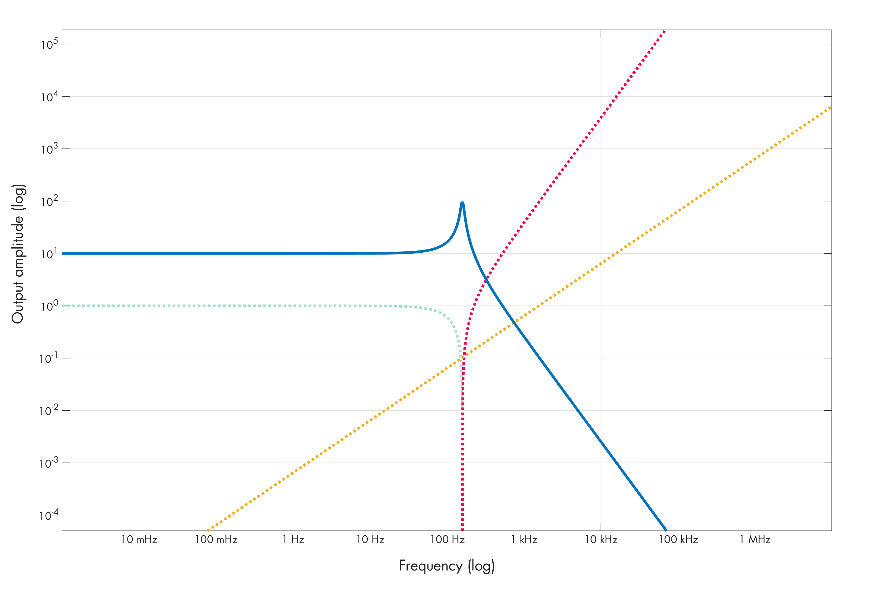
Instead of a flattened section, we get a spike — a Q factor higher than 1, implying a gain at the crossover frequency.
There are no values of R1, R2, C1, and C2 that would result in the curves being positioned like this for our passive circuit, but remember that spike. We’ll come back to this shape soon!
Back to the real world
The calculation reveals just one way to keep the circuit working as expected: to keep the Im(Ca) line as low as possible, we need to minimize its constant multiplier for f — R1·C1 + (R1 + R2)·C2 — without impacting the multiplier for Re(Ca) to the same extent. The best option is to keep C2 ≪ C1 and R1 ≪ R2 — i.e., make the second stage much higher impedance than the first. Alas, while this is doable for two stages, the approach quickly becomes impractical as the number of filter stages goes up.
An obvious solution is to add op-amps configured as voltage followers in between the filters. This isolates the sections from each other, prevents the formation of parasitic filters, and keeps the math clean no matter which values of R and C you choose for each stage:

The frequency response of properly isolated, chained RC lowpass filters is shown below:
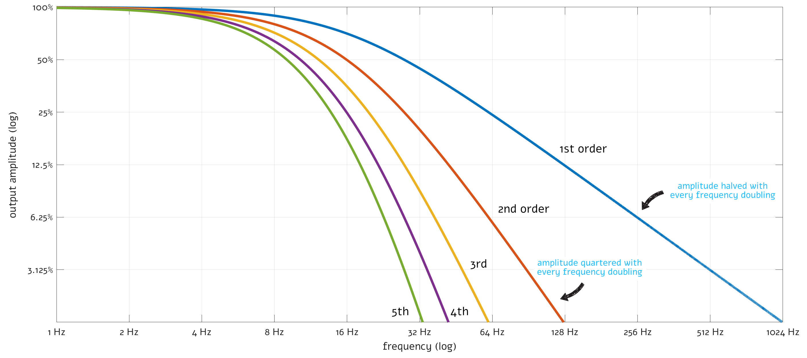
The approach works, but one problem remains: no matter how many RC filters we stack, there’s still a pronounced bend in between the bandpass and bandstop portions of the curve. In all cases, the center frequency, defined as the midpoint of the bend, is the same — fc = 1/2πRC. That said, as noted earlier, the attenuation at fc is raised to the power equal to the number of stages. Two stages reduce the amplitude to 50% (Q = 0.5); four stages push it down to 25% (Q = 0.25). Meanwhile, the customary “cutoff” point — corresponding to an amplitude of ~70% — keeps inching toward DC.
To fix this, we need more powerful sorcery.
Paging doctor Sallen-Key
Recall from the earlier article that standard analog filters behave correctly in the special case of a steady sine wave. For radio, this works because the carrier signals are near-perfect sines that are modulated at a comparatively glacial pace. For audio, the filters don’t actually do what we assume — but their effects sound natural because they mimic real-world acoustic phenomena.
And so, if you’re a filter designer concerned only with steady sine waves, there is a simple (if seemingly deranged) solution to the issue at hand: just make the circuit slightly resonant around fc. If we can get that waveform to constructively interfere with a reflected or looped-back version of itself, we get a localized spike in “loudness” — and turn that ugly curve into a nice, pointy knee. Sure, interesting things will happen if the input waveform doesn’t resemble a sinusoid — but most of the time, the trick works every time!
There are many ways to build resonant circuits, but a particularly clever and low-component approach is known as the Sallen-Key topology. The lowpass version can be derived from a familiar, passive second-order RC filter paired with an output-side voltage follower; the starting point is:
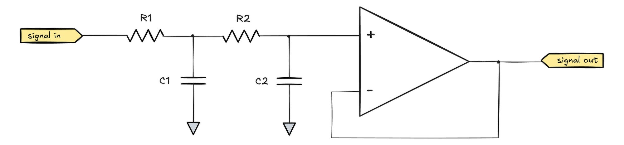
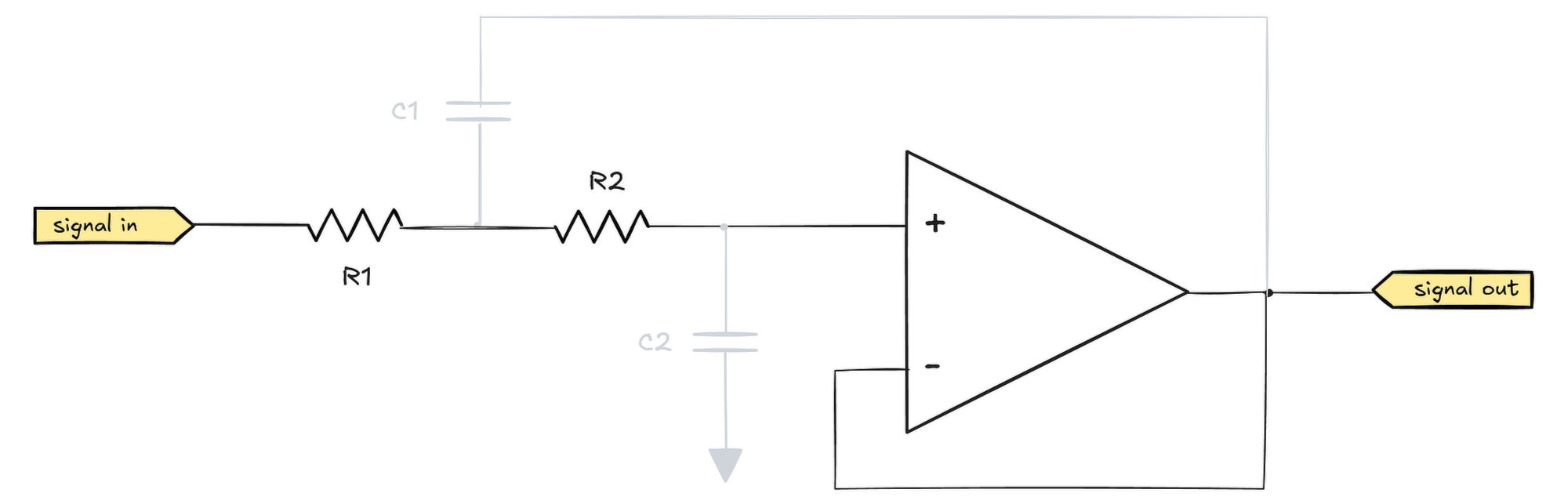
To turn this into the actual Sallen-Key topology, the first capacitor is disconnected from the ground, and hooked up to the output of the voltage follower:

The modification is not obvious, so let’s analyze it starting with the case of a low-frequency input signal. As we approach DC, both capacitors will exhibit high impedance, so the circuit’s output voltage will be predominantly influenced by the signal path through the two resistors. The op-amp doesn’t appreciably load its inputs, so the resistors do nothing, and Vout must be approximately the same as Vin. In effect, we have a voltage follower with 1x gain:
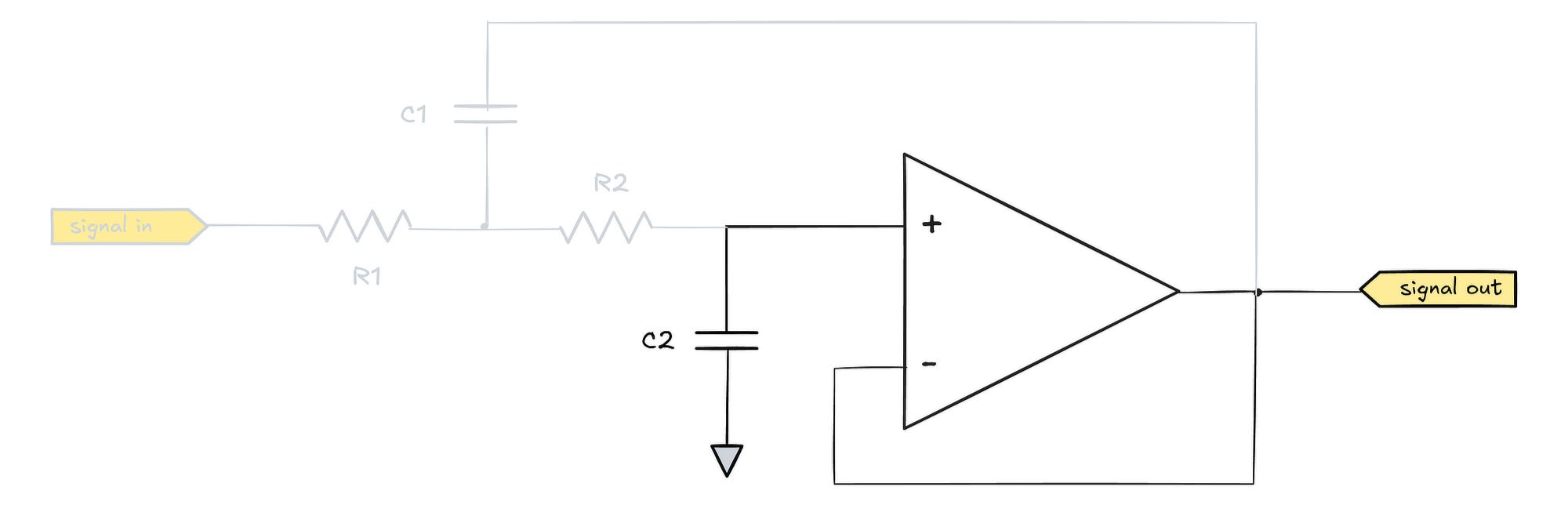
Conversely, at high frequencies, C2 has a very low impedance compared to R2; in effect, any input signal should be more or less shunted to the ground, and the output should sit around zero volts:
So far, we seem to have a pretty standard lowpass filter. But next, let’s consider some midpoint frequency where the impedance of C1 is comparable with that of the signal path via the resistors, and isn’t yet dwarfed by the C2 shunt. At a given frequency not far from that midpoint, the equivalent circuit might be visualized this way:
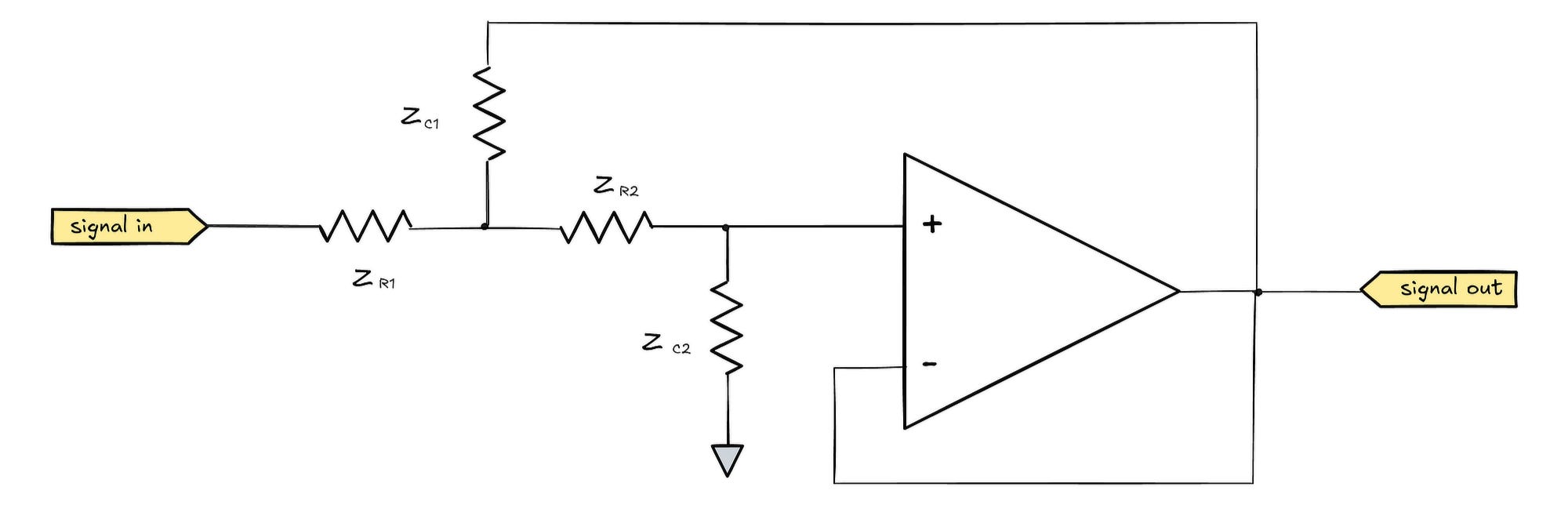
What’s that? Yes, it’s a positive feedback loop that constructively adds the output signal onto the input! Critically, this feedback loop vanishes the moment we get sufficiently far away from fc, instead reverting to one of the two scenarios we discussed before.
This is pretty cool. The amount of feedback is controlled by the ratio of component values, and is usually expressed using the Q factor — a now-familiar value representing the amplitude boost at fc. The filter’s frequency response for various Q factors is shown below:
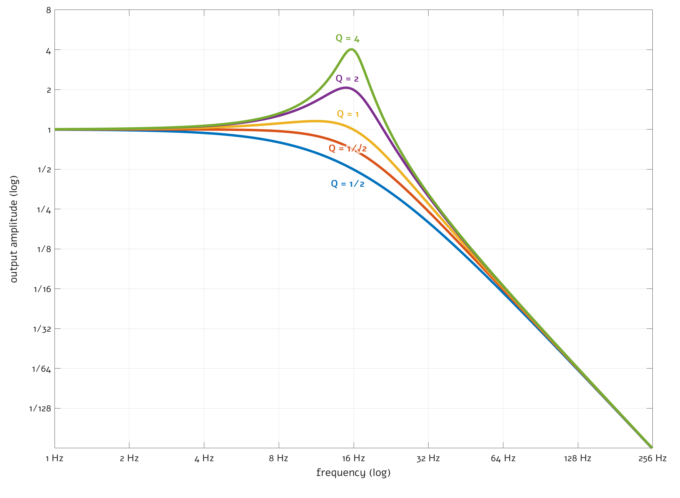
As discussed earlier, at Q = ½, the curvature is identical to the optimally-designed non-resonant second-order RC filter. At Q = √½, we get a maximally flat response without any overshoot. At Q = 1, a tiny bit of ripple is present on the low-frequency side. Finally, at higher Q factors, the ripple becomes profound and is present on both sides of fc.
The formulas for this filter’s center frequency is the same as for the passive second-order RC filter we talked about before. It corresponds to 50% (-90°) phase shift and is given as:
In the same vein, the following is the formula for the Q factor:
This one differs from the formula for the earlier passive RC filter, precisely because of the addition of a feedback loop.
In practice, we don’t need this many degrees of freedom in circuit design. In particular, the filter can be built with two identical resistors (R) and two complementary capacitances centered around a common midpoint (Cref):
This greatly simplifies the math:
With these constraints in place, we can pick R and Cref to dial in a specific center frequency (and perhaps the desired input impedance or noise floor). Next, we simply pick n for the desired Q factor, and calculate the capacitances: C1 = Cref ⋅ n and C2 = Cref / n.
…but at what price?
Well, right. Resonant filters are a special can of worms. The distortion introduced by non-resonant RC filters can be problematic, but is also fairly localized and easy to model. For example, a non-resonant lowpass will just round the edges of a square wave:
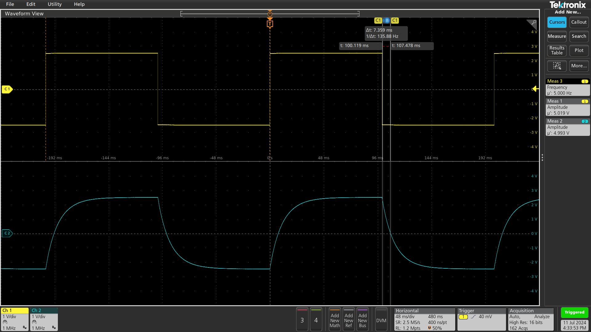
Resonant filters, on the other hand, essentially turn into (damped) oscillators when presented with an input pulse. The following oscilloscope trace shows profound ringing in response to square wave spikes (at Q = 5):

Of course, analog filters can be designed to have more complex frequency responses, impulse responses, phase characteristics, and so on; digital filters don’t even need to operate in the sine-wave domain. But the design process always involves balancing some really messy trade-offs; a perfect, universal signal filter simply doesn’t exist.
👉 For a thematic catalog of articles on this blog, click here.
I write well-researched, original articles about geek culture, electronic circuit design, and more. If you like the content, please subscribe. It’s increasingly difficult to stay in touch with readers via social media; my typical post on X is shown to less than 5% of my followers and gets a ~0.2% clickthrough rate.
There is an amusing anecdote in *The Art of Electronics:* a purely RC circuit *can* actually produce a voltage gain greater than one. Thought it was worth mentioning considering your earlier mention of Q>1 with RC.
https://electronics.stackexchange.com/questions/242901/passive-rc-network-with-voltage-gain-greater-than-unity
I tend to reserve the term “distortion” to nonlinear effects. Everything you have described here is perfectly linear as long as you don’t approach clipping.
Yes. the impulse response may look gnarly in the time domain, but that’s mostly an inherent time/frequency effect. .