
Negative resistance
Hello! The blog you’re trying to reach is currently unavailable. I am Skippy, your friendly blog assistant. How can I help you today?
> quit
I’m sorry. This function is currently available only to Skippy Premium and Premium+ subscribers. Would you like to talk about ✨ negative resistance instead?
> nope
I’m sorry. This function is currently available only to Skippy Premium and Premium+ subscribers.
Welcome. Welcome again. If you tinker with analog electronics, you might have heard that some circuits can exhibit negative resistance. This is usually followed by a current-to-voltage plot featuring some sort of a kinked curve and an assertion that this property might help the circuit designer in some way.
But what does it mean, exactly? The concept of negative resistance is interesting, counterintuitive, and explained on Wikipedia in a rather rambling way. If you’re up for it, I think we can do better than that.
The article assumes familiarity with voltage, current, and the behavior of operational amplifiers. If you need a refresher, start with this primer, then read up about transistors here and signal amplification here.
Defining resistance
As a quick recap, resistance (R) can be understood as the opposition to the flow of steady current through some portion of the circuit. The quantity describes the relationship between the applied electromotive force — that’s voltage — and the amount of charge moving per second (that’s current).
In contrast to some other phenomena in electronic circuits, resistance is not inherently dependent on time or signal frequency. If you know the voltage (V) applied to a purely-resistive component, the current (I) flowing at that exact moment is simply:
In resistors, the parameter remains constant across a wide range of operating conditions. This means that if we plot I in relation to V, we get a straight line that crosses through the center of the coordinate system. The slope of the line depends only on the component’s resistance:
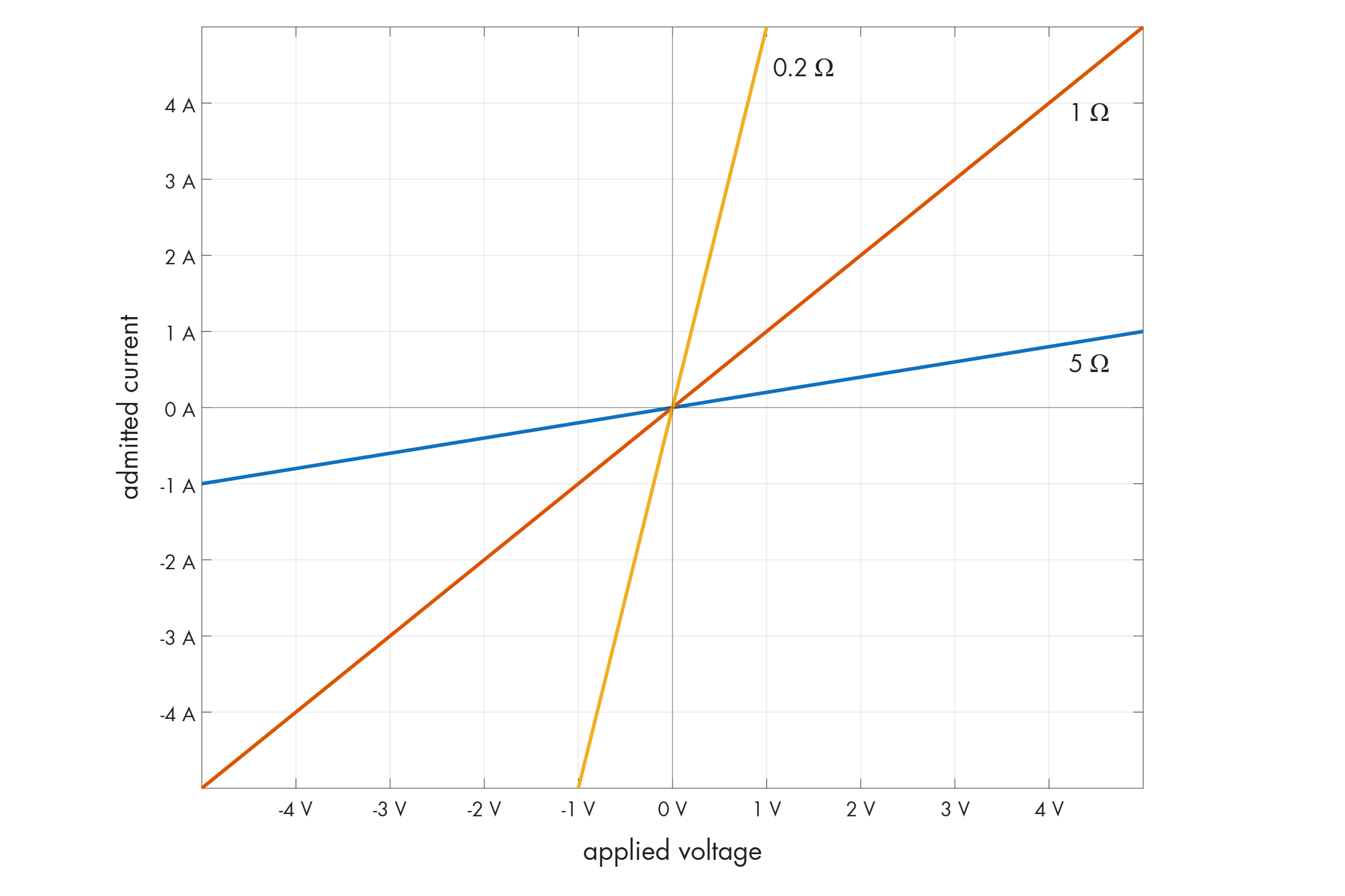
For example, in a 5 Ω resistor (blue line), the current is 200 mA if the voltage across the terminals is 1 V, rising to 1 A if the electromotive force increases to 5 V.
Some other components, such as diodes and transistors, oppose the flow of current in a manner that depends on the applied voltage. We can still model their behavior using the concept of resistance, but we don’t get a constant reading. In an earlier article, I provided a V-I curve for a small diode; if we take these measurements and calculate the effective R by rearranging the earlier equation (I = V / R ⇒ R = V / I), we obtain the log-scale V-to-R plot shown on the right:
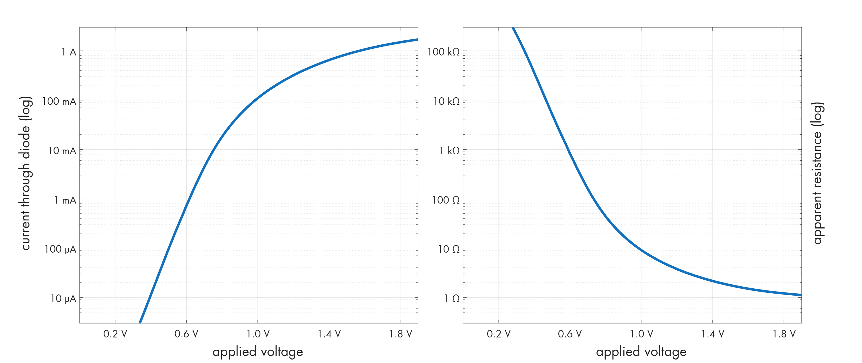
For a chosen point of the V-I curve, we can also calculate so-called differential resistance. This parameter doesn’t tell us anything about the overall relationship between voltage and current; instead, it models the relative response to small deviations from the chosen baseline. For example, in the vicinity of 1.2 V on the plot above, the slope of the V-I curve is such that a change of Δv = +/- 10 mV causes the current to change by Δi = +/- 20 mA. If we divide Δv by Δi and squint our eyes hard enough, we can say that the “local” resistance is 500 mΩ. Again, that number has nothing to do with the bulk resistance of the diode at 1.2 V, but it’s a useful abstraction for modeling what happens to small signals that are piggybacking on top of a constant bias voltage.
In physical terms, resistance is associated with the consumption of energy. We’re making an effort to push charges through; some of the energy is absorbed by the medium and then taken out of the picture — turned into heat, light, motion, or captured in chemical bonds.
To model these dynamics, we need to tap into the official definition of voltage. It’s the amount of energy (E, in joules) we’re willing to expend to move the unit of electrical charge (Q, in coulombs, equal to about 6.2 quintillion electrons):
We also need the definition of current; as noted earlier, it’s the amount of charge that’s moved per second through a point in the circuit:
We can rearrange the second equation to solve for Q (Q = I · t), and then shuffle the first one to solve for E (E = V · Q). Combining these forms, we get E = V · I · t.
Finally, we tap into the physical definition of power (P, watts); it’s the rate at which energy is expended:
If we plug the earlier E = V · I · t formula into the fundamental power equation, we obtain:
That’s to say, the amount of electrical power consumed by an electronic circuit depends on the supplied voltage, the resulting current, and nothing else. For resistive circuits, we can further substitute I = V / R and get:
So, a resistive element consumes energy provided by the power supply at a rate that’s proportional to the square of the applied voltage, and inversely proportional to the component’s resistance. For example, a 220 Ω resistor subjected 10 V will dissipate about 455 mW as heat.
True negative resistance
This brings us to an interesting question: what would it mean for a component to have a resistance of less than 0 ohms?
Well, we can start by stating the obvious: if R is negative and I = V / R, then the current-to-voltage plot will have a downward slope. For example, for R = -5 Ω, we’d get the following:
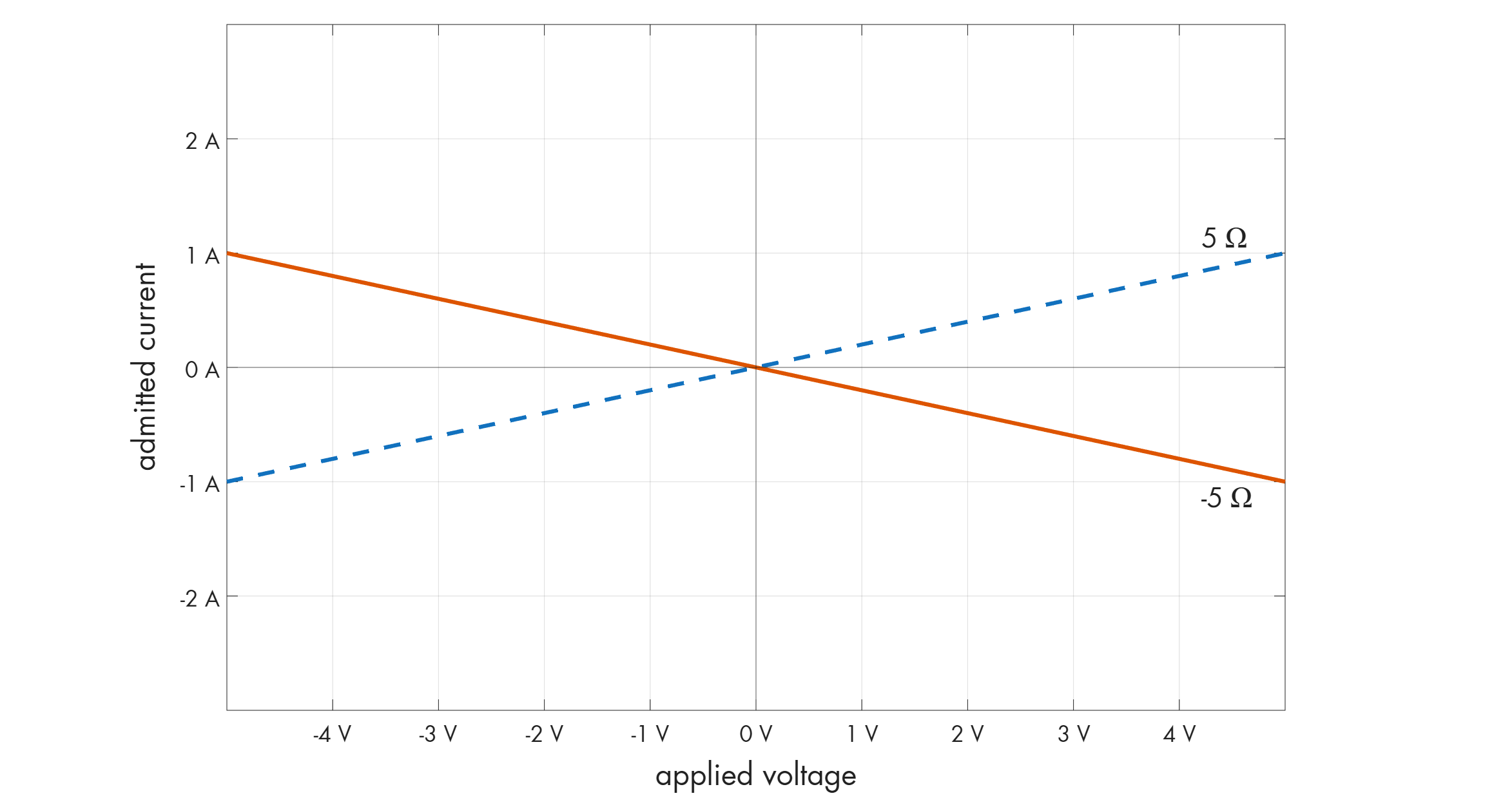
It would appear that if we apply a positive voltage to a “negistor”, we should get a current that’s proportional to the voltage but with an opposite sign. The natural flow of conventional current is from the more positive side to the more negative one, but in this instance, it must be flowing the other way round.
Alas, a negistor can’t exist unless it’s equipped with an external power source. Recall our derivation of the power dissipation formula: P = V2 / R. In this equation, if R is negative, so is the consumed power. This implies that the component would need to extract energy from its surroundings and put it back into the circuit.
On the other hand, if we allow an external power supply, a circuit with constant negative resistance can be constructed pretty easily:
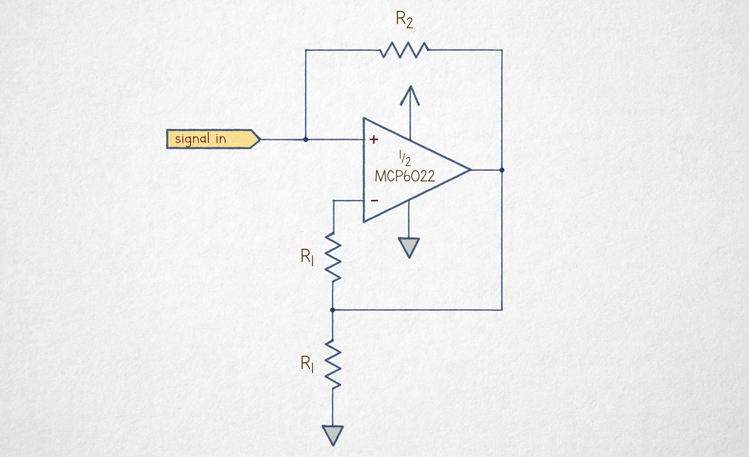
If you’re rusty on operational amplifiers, now would be the time to revisit an earlier feature on this blog. Otherwise, the analysis can be simplified by assuming that R2 is large enough so that both the op-amp output pin and the signal source can supply worst-case currents via this resistor without causing the voltage to sag.
This assumption allows us to ignore R2 for the initial part of the analysis: on a voltage basis, the circuit is just a conventional non-inverting amplifier with the gain determined by the bottom R1-R1 voltage divider. You can find the derivation of the circuit’s gain in the linked article, but the bottom line is that if the resistors are the same, then the amplifier’s Vout ≈ 2 · Vsignal.
We can now come back to R2: the left terminal of the resistor is connected to Vsignal while the right terminal sits at Vout ≈ 2 · Vsignal. From this, we can apply the fundamental I = V / R formula to calculate the current flowing through:
This current must be flowing into or out of the signal source because there’s nowhere else for it to go: the input of the op-amp has a very high impedance.
The placement of the minus sign is inconsequential, we can also rewrite the equation as:
In other words, the circuit behaves the same as a negative resistance -R2 placed between Vsignal and the ground. We can confirm this on the following empirical V-I plot, captured for R2 = 220 Ω and a supply of 5 V:
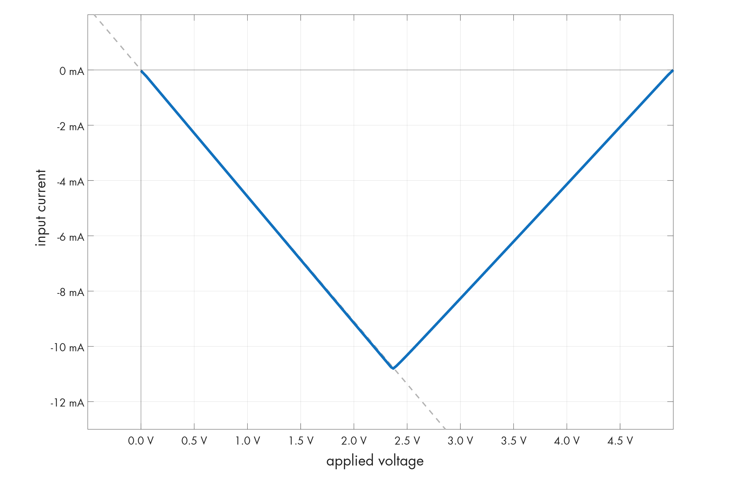
The circuit does nothing at Vsignal = 0 V, but as the voltage increases, it backfeeds more and more current into the signal source.
The plot also exposes a major shortcoming of this design: because the process depends on keeping one terminal of the resistor at 2 · Vsignal, we eventually run out of range; in a 5 V circuit, this happens around 2.5 V. Past that point, the op-amp is maxed out and the voltage across the terminals of R2 begins to decrease; so must the reverse current, eventually reaching zero at 5 V.
Negative differential resistance
The arrangement discussed earlier has some niche uses, but most of the time, “negative resistance” is a reference to a somewhat different phenomenon: a V-I curve that looks normal in parts, but has a section with a downward slope.
The simplest example of this phenomenon is a situation where, past a certain point, an increase in voltage causes a relative constriction of the admitted current. A model of this behavior is shown on the left:
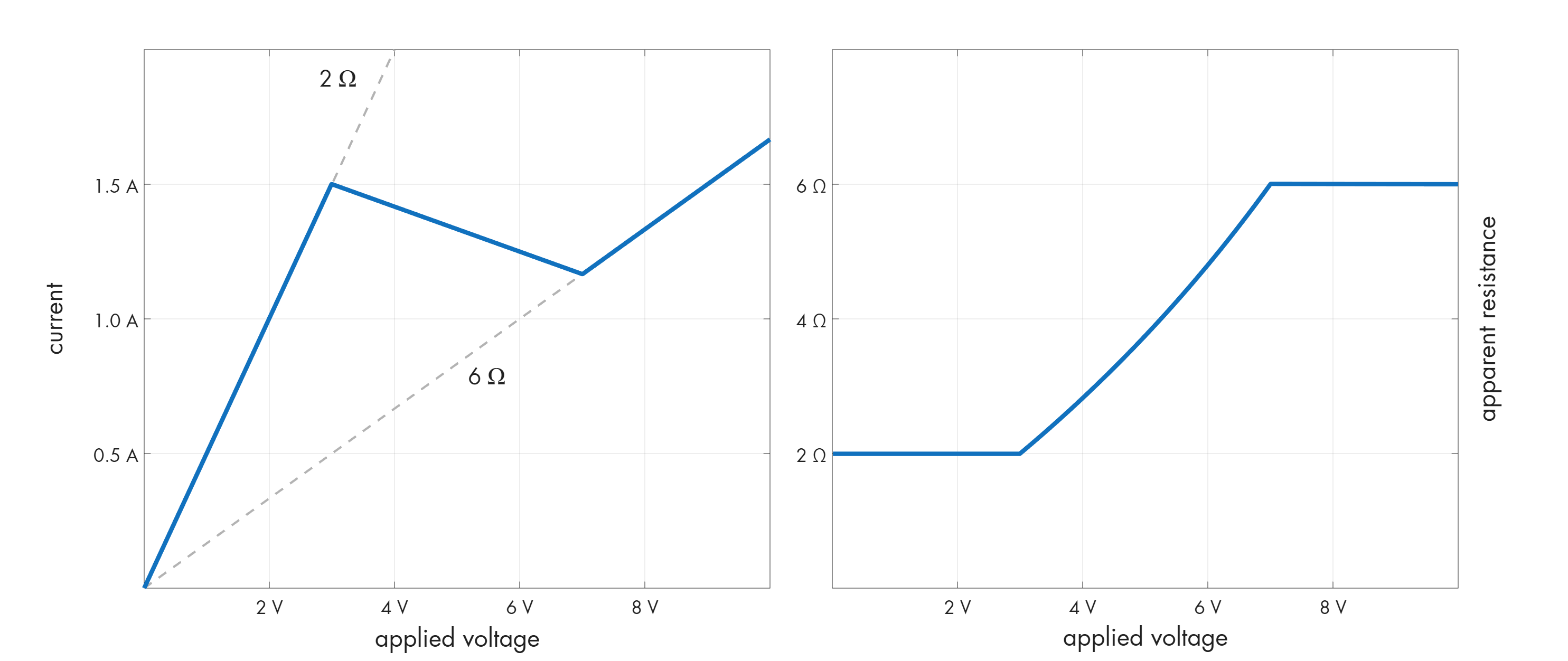
This inverted section is called negative differential resistance (NDR). At first blush, the term makes no sense: if you look at the plot of voltage to computed resistance on the right, the apparent resistance stays positive (and in fact, goes up). To make sense of the terminology, recall the idea of calculating differential resistance as the “local” ratio of step change in voltage to step change in current: r = Δv / Δi. In the downward portion of the V-I curve, Δv > 0 while Δi < 0, so the differential value is negative. But really, a simpler mnemonic is just that it’s an inverted slope.
At the same time, because “real” resistance remains positive, such V-I kinks can manifest without the need for an additional power supply. An easily-constructed example of a negative differential resistance is the following arrangement of two complementary JFETs:
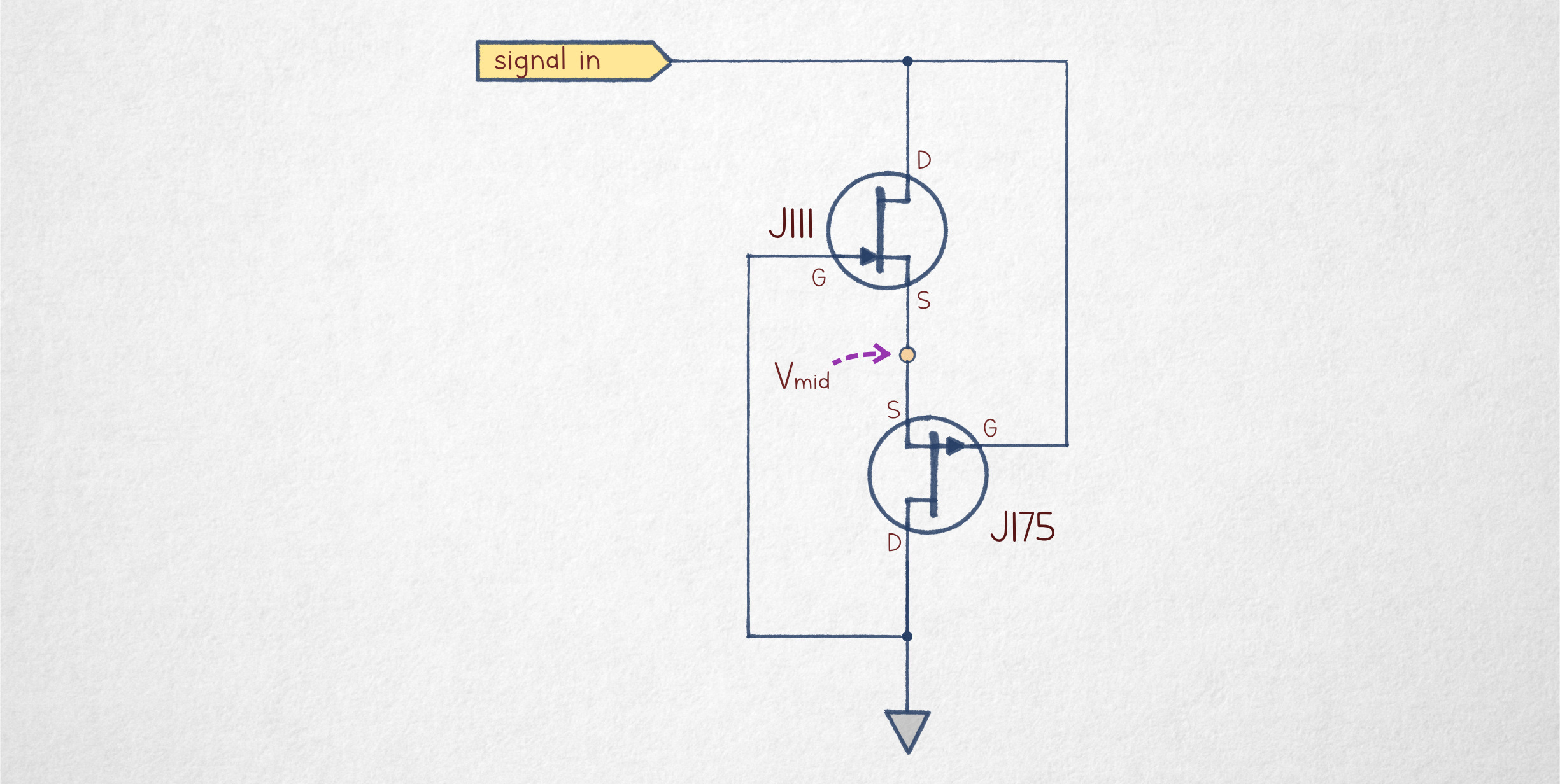
This circuit, known as the lambda diode, should be fairly easy to understand if you’re familiar with the behavior of junction field-effect transistors; if not, a quick refresher can be found here. In a nutshell, the JFET drain-source path is conductive by default, but the flow of current can be constricted by making the gate-source voltage difference (VGS) sufficiently negative in n-channel devices, or sufficiently positive in p-channel ones. In this circuit, the cut-off point is around VGS = -4 to -5 V for the n-channel transistor (J111) and VGS = +4 to +5 V for its p-channel counterpart (J175).
To simplify the analysis, let’s assume that the transistors have identical characteristics except for the polarity of the gate voltage; that is, let’s say that the top one conducts exactly as well at VGS = -2 V as the bottom one conducts at VGS = +2 V. That assumption is not quite true, but it’s good enough for a qualitative result.
Next, let’s use Vmid to denote the unknown voltage at the midpoint of the circuit (as marked in the schematic) and note that the gate of the n-channel transistor is wired to the ground. With this in mind, we can express the gate-source voltage delta for the top JFET as:
The bottom transistor has its gate hardwired to the positive supply, so the corresponding formula is:
The transistors are connected in series, so the same current must be flowing through both. This current is decided chiefly by VGS, and we’ve made the assumption that both JFETs have the same characteristics except for the flipped sign for the gate voltage. So, equal currents would call for VGS (bottom) = -VGS (top), which further expands to:
This puts the transistors’ VGS at half the input voltage, priming both to cut off once the input voltage crosses about 8 V.
And indeed, we can see this on the following empirical plot:
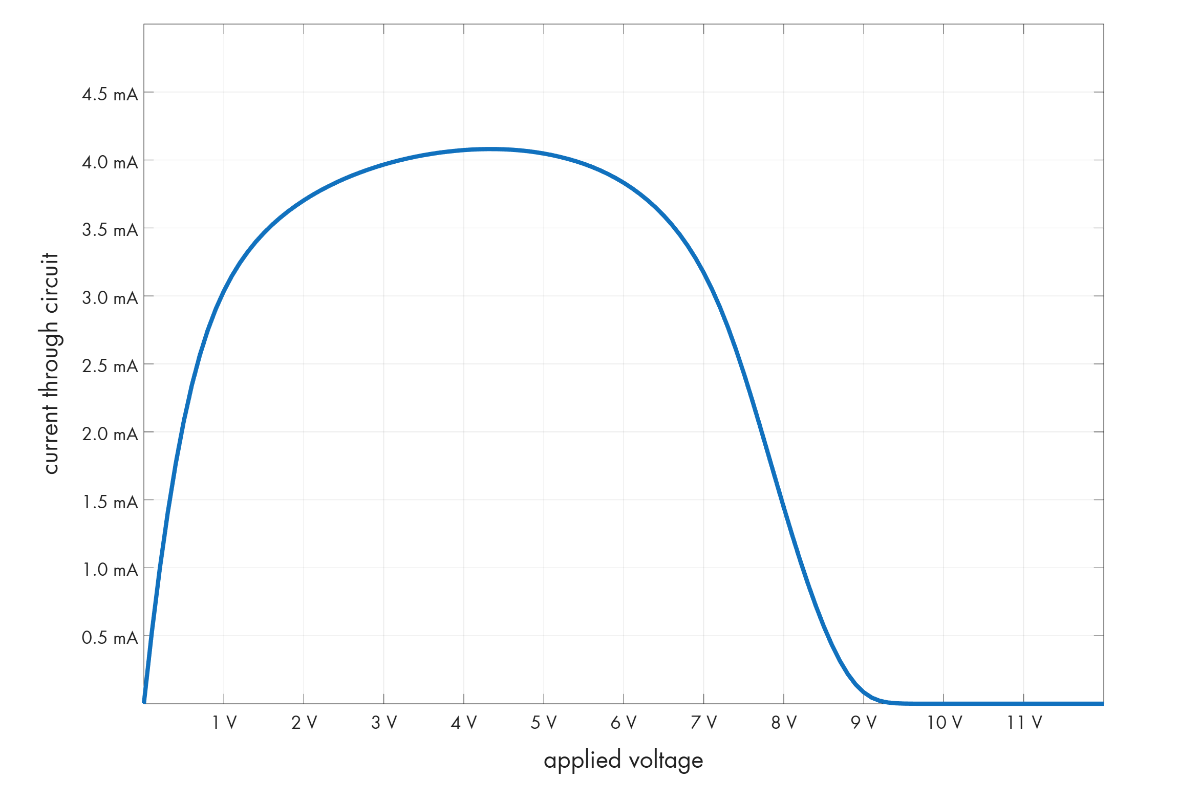
In the lambda diode, the current decreases as the voltage rises from about 6 to 9 V.
Another flavor of negative differential resistance can arise if we’re supplying a controlled current to some circuit, but past a certain point, by some mechanism, the voltage needed to sustain it takes a nosedive. A conceptual illustration of this effect can be found below:
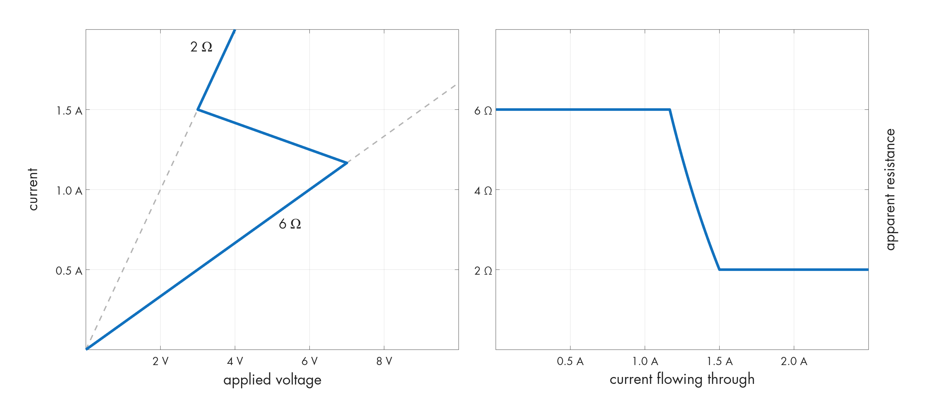
In this plot, the circuit behaves like a 6 Ω resistance up to a point, but then “snap backs” in the horizontal axis; currents above about 1.2 A can be apparently sustained with a markedly lower applied voltage.
This scenario is qualitatively different from what we’ve talked about before; in the earlier V-I plot, there were multiple voltages that could produce the same current. In the snapback scenario, we have multiple currents that can be sustained by the same voltage.
As it turns out, you can get that behavior out of a single bipolar transistor; we talked about an example of a circuit exhibiting this behavior in an earlier article on this blog:

Error code 400: daily token limit exceeded. Higher limits are available to Skippy Premium and Premium+ subscribers.