
MCU land, part 4: building an audio toy
Using ADCs, DACs, and external memory on an 8-bit AVR chip.
In a recent series of articles, I sought to demystify the world of “bare” microcontrollers and promote them as a viable alternative to Linux-based embedded solutions such as Raspberry Pi. In today’s post, I’d like to offer an walkthrough of an audio processing project implemented on a bottom-dollar 8-bit MCU.
The design is a whimsical toy I built for my youngest son. Pressing one button allows him to record up to 10 seconds of audio; the other four buttons play back the recording normally, in reverse (spooky!), or at 2x or 0.67x speed (for a “chipmunk” and a “grownup” voice):
The toy itself is obviously silly, but it’s a good demonstration of the strengths and limitations of the AVR DA series chips.
Microphone input
The microphone sub-circuit is a straightforward application of an inverting operational amplifier:
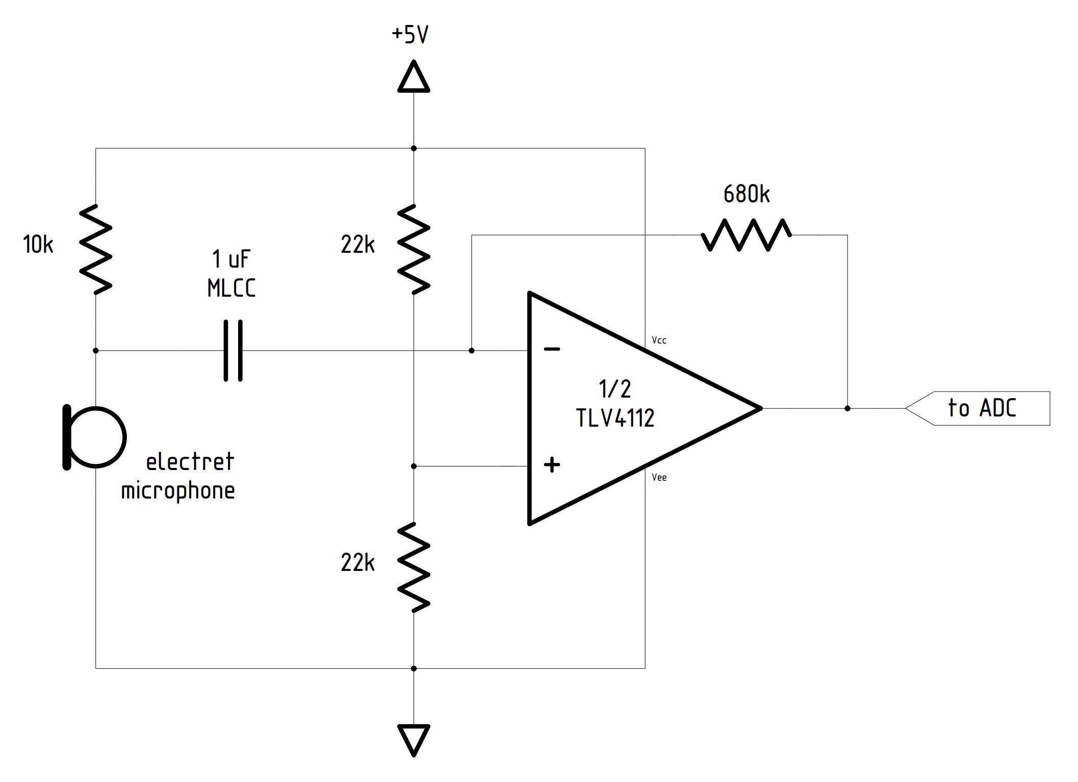
An op-amp can be thought of as a voltage comparator. If the voltage on its non-inverting (“+”) input is higher than on the inverting (“-”) leg, the output goes high. If the inverting input becomes more positive, the output goes low. If the voltages are the same, the output is at a midpoint.
Here, the non-inverting input is always held at Vcc/2 because it’s connected to a voltage divider. As for the inverting leg, in the circuit’s steady state, the 1 µF capacitor prevents the flow of current, so the voltage here simply tracks the output voltage via the 680 kΩ resistor. This forms a negative feedback loop: if the “-” leg falls below the “+” one, the output voltage increases, in turn pulling the leg back up. The opposite is also true - so simplifying a bit, the only stable equilibrium is: output = non-inverting input = Vcc/2.
The situation changes if there’s an alternating signal on the other side of the DC-blocking capacitor. This change in potential momentarily allows some current to flow through the cap. Critically, the AC impedance of that path is much lower than the impedance of a 680 kΩ resistor, so the op-amp must swing its output voltage proportionately more to induce a matching current through the resistor and bring the inverting input back in line. Voila — a robust microphone amplifier.
Since this is a transimpedance op-amp circuit — that is, an arrangement that converts current to voltage — it is unnecessary and counterproductive to include a resistor in series with the capacitor. From Ohm’s law, the current-to-voltage ratio is determined by the single feedback resistor. There are many confused or overly complicated takes on microphone amplifiers on the internet; for an authoritative discussion, look no further than this document from Texas Instruments.
The 680 kΩ resistor might need to be lowered if using a more sensitive microphone or working in a noisier environment. The op-amp can be freely substituted, as long as the replacement is capable of rail-to-rail output, can run off 5 V, and has a gain-bandwidth product of at least around 3 MHz. Other sensible choices include TLV271, MCP6021, and OPA2322; the last two are particularly suitable for higher-fidelity microphone amplifiers.
Speaker output
Digital audio processing typically involves an analog-to-digital converter (ADC) that quantizes voltage levels into bits; and a complementary digital-to-analog converter (DAC) that later turns the data back into a continuum of voltages. Alas, most DACs have high-impedance outputs — that is to say, they can’t deliver substantial currents needed to operate a speaker.
To address this problem, I opted to use the second op-amp in the dual TLV4112 package to build what’s known as a voltage follower. Recall the earlier discussion of how, with a feedback loop in place and no microphone signal present, the output of our op-amp mirrored the voltage supplied on the non-inverting leg. We can use this principle to obtain a faithful 1:1 reproduction of the DAC signal, but bless it with the TLV4112’s 300+ mA output current capacity:
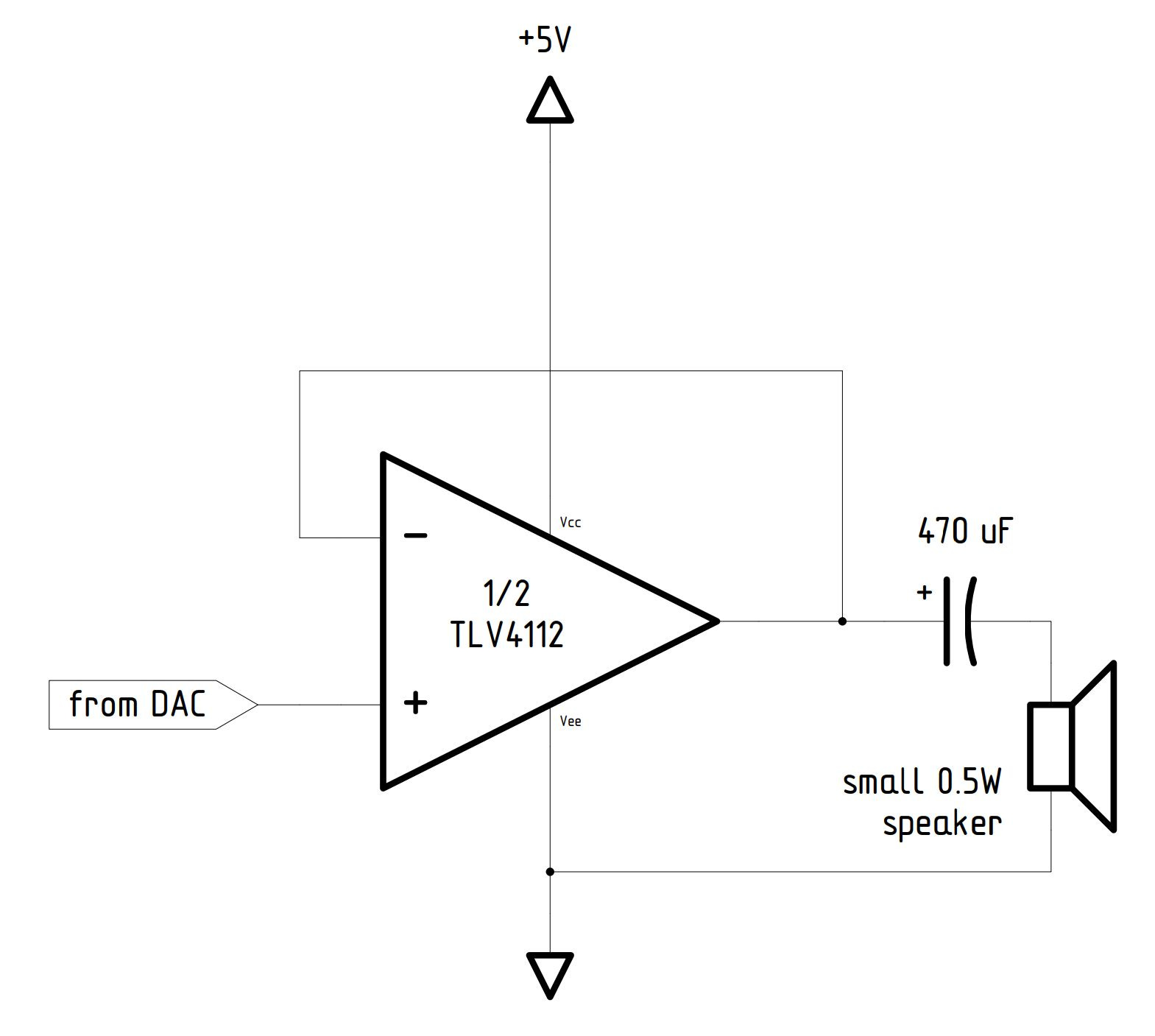
The purpose of the capacitor is to prevent a steady-state current through the speaker, which would waste battery battery power and perhaps cause the op-amp or the speaker to overheat. The capacitor is large enough so the highpass filter formed together with the 8 Ω speaker lets through most audible frequencies. The formula for the RC filter cutoff frequency is 1/(2πRC) — or, in this case, a bit under 50 Hz.
As far as IC substitutions go: speaker-side op-amp can have modest bandwidth, but needs to have rail-to-rail output and at least 200 mA output capacity. Reasonable alternatives include AD8531, AD8532, MAX4230, etc.
The digital domain
The digital circuit is uncomplicated. Analog-to-digital and digital-to-analog converters are included on the die of the AVR128DA28 MCU, so the only major peripherals are a memory chip and a couple of switches mounted on the PCB:

The external memory is a 128 kB SRAM module from Microchip (23LC1024), operated via the Serial Peripheral Interface (SPI) bus. I talked about this exact chip and the SPI protocol in an earlier article, so I’ll omit the details here. Suffice to say, the communication scheme is exceedingly simple and partly automated by the MCU.
The lines connecting to the switches sport configurable ~30 kΩ pull-up resistors on the microcontroller die, so there is no need for external biasing; pressing the button simply provides a low-impedance path to the ground and produces a logical zero on the corresponding pin.
There is a small analog lowpass RC filter visible on the left and connected to PD7 (AREFV). This is because the converters inside the MCU need a stable voltage reference, but the on-die voltage bus fluctuates in response to inrush currents needed to operate the SPI bus. Depending on I/O timing, this can produce anything from a subtle hiss to a loud squeal. An external, filtered reference signal helps avoid the mess.
The software side
With no operating system facilities at their disposal, developers working with bare MCUs sometimes need to devise custom ways of parallelizing or carefully timing series of operations in their code.
The most straightforward option is a synchronous event loop that iterates over a fixed sequence of steps, such as checking keyboard input, performing computations, and updating the screen. An event loop is a viable choice for audio processing, but it is inherently hacky, because sampling rates can be thrown off by changes to unrelated portions of the code.
A more flexible if perilous approach is to leverage hardware interrupts: that is, having the MCU periodically stop what it’s doing, save the current execution state, and then temporarily pass the baton to a custom interrupt service routine (ISR). Interrupts can be driven by timers, I/O events, or certain CPU states. Their peril has to do with the occasional concurrency and code reentrancy issues that catch inexperienced developers off guard.
In my implementation, I’m relying on the TCA0 clock interrupt, configured to fire at the frequency of 10 kHz. The ISR does most of the heavy lifting: it queries the ADC, streams the data to and from the SRAM module, and forwards samples to the DAC. There is a minimal event loop running in parallel, tasked with reading button states and passing that information to the ISR.
The added perk of this design is that very little is needed to implement slowed-down and sped-up playback: the main event loop simply changes the interrupt frequency ahead of requesting audio, tweaking it from the nominal 10 kHz to either 6.7 or 20 kHz.
Other implementation details are probably not worth dissecting in great detail; for example, the ADC and DAC interface on these MCUs is trivial, and a readable walkthrough can be found in the richly-annotated source code for this project.
Practical limitations
Despite its unserious nature, the project is a reasonable introduction to digital signal processing on dirt-cheap MCUs; I am fairly certain that the orange “record” button, retailing for $3.50, is the most expensive part of this build.
For the most part, I’m not pushing the chip to its limits: the code uses less than 2% of the microcontroller’s available program memory and operates at a fraction of the maximum CPU speed. The most significant constraint is sample storage: even at the subpar 8-bit resolution and 10 kHz sample rate, the MCU’s built-in SRAM can only hold 1.6 seconds of uncompressed audio. The device offers the ability to overwrite the unused sections of its program memory, so one could theoretically abuse this to get another 100+ kB for “free”. That said, the extra 128 kB SRAM chip used in this project costs $2.50, while a slightly less power-efficient 8 MB DRAM module, APS6404L-3SQN, retails for $1.60. In other words, the hacky solution is probably not worth the time.
The analog frontend also shows some limitations. Perhaps most notably, onboard ADCs and DACs are inherently vulnerable to digital noise originating within the chip — a problem mitigated here with the AREFV approach, but certainly not solved to the satisfaction of an audiophile.
Sample resolution would be a challenge in more serious applications, too: the ADC on the AVR DA has a maximum resolution of 12 bits, well short of the 16-bit baseline for HD audio. The ADC supports sampling at up to 130 kHz, so one could accumulate multiple samples and do some averaging; that said, a standalone audio-grade ADC, such as PCM1808, might offer an easier way out.
A similar constraint exists on the output side: the maximum resolution of the built-in DAC is 10 bits. Better resolution can be achieved by updating it at a higher frequency and smoothing the output with a low-pass capacitor; that said, once again, a standalone DAC might be a simpler route — and in that category, PCM1780 is a reasonable pick.
👉 Check out the next article in the MCU programming series: Cortex-M7 IRQ and chill. To learn more about ADCs and DACs, try this link. To review the entire series of articles on digital and analog electronics, visit this page.
I write well-researched, original articles about geek culture, electronic circuit design, algorithms, and more. This day and age, it’s increasingly difficult to reach willing readers via social media and search. If you like the content, please subscribe!
For a variant put together by a reader, check out: https://twitter.com/rgerganov/status/1623000100229328898
I believe it's based on an earlier revision that I shared on Twitter & Mastodon, but the fundamental approach is the same.
One-part schematics here: https://lcamtuf.coredump.cx/soft/playback.pdf