In one of the earlier articles on electronics, I professed my love for perfboards and through-hole prototyping. It’s not a matter of nostalgia; I simply enjoy being able to crank out circuits at a moment’s notice. Surface-mount technology offers many benefits, but it calls for custom-order circuit boards that take 1-2 weeks to arrive. The wait is particularly frustrating if you’re trying to iterate on a new design.
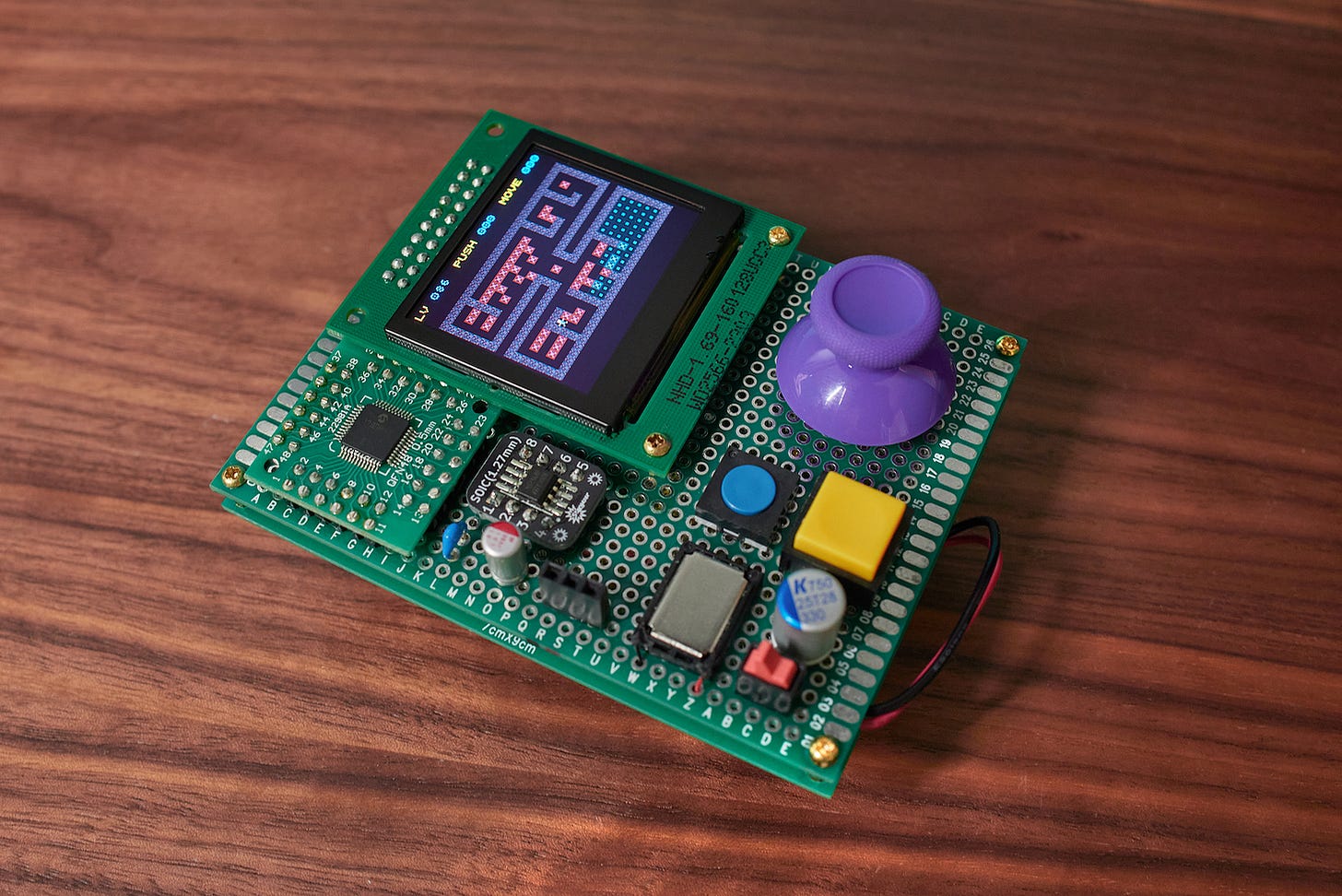
Of course, the perfboard approach has drawbacks too. For one, it is time-consuming to assemble more than one prototype. Just as importantly, the final product isn’t as polished as a factory-made board: it’s probably not something you’d sell on Kickstarter or gift to a friend.
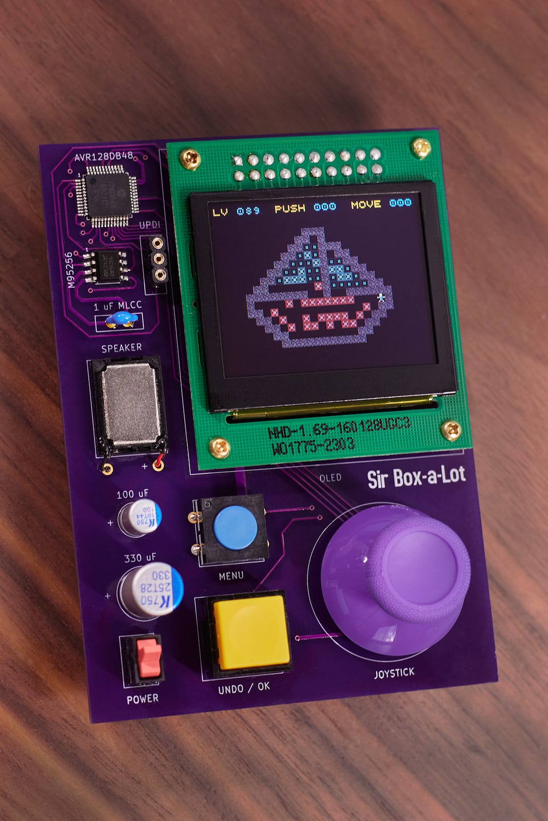
Luckily, once you have the circuit figured out, designing a printed circuit board (PCB) is not hard. To illustrate, let’s take my earlier perfboard project — Sir Box-a-Lot — and let’s make it worthy of a Kickstarter campaign!
Step 1: part footprints
When it comes to hobby PCB design, there is no contest: the gold standard is KiCad, a multiplatform open-source tool originally developed by Jean-Pierre Charras. It is the best choice unless you’re ready to pay three to four figures for a commercial tool.
The centerpiece of KiCad is its PCB Editor module, which allows you to place two-dimensional footprints of various components on the screen, manually arrange electrical connections, and then add silkscreen annotations to the PCB. But before you can do anything with that, you need to procure footprints for all the components that are used in your project to begin with.
KiCad comes with an extensive library of footprints, but the data covers just a small fraction of the parts in stock at Mouser or Digi-Key. For this project, I could find a generic TQFP-48 footprint for the AVR MCU (“TQFP-48_7x7mm_P0.5mm”) and a SOIC-8 footprint for the EEPROM chip (“SOIC-8_3.9x4.9mm_P1.27mm””); but I had no luck with the OLED module, the switches, or the speaker.
Luckily, adding your own footprints is a breeze: they usually consist of not much more than a couple of soldering pads or holes placed on a fixed grid (2.54 mm for most through-hole components, between 0.5 mm and 1.27 mm for most surface-mount stuff). The pads can be accompanied by a rectangle or a circle to mark the outline of a part, and perhaps some text to assist with manual assembly.
KiCad footprints are created in the Footprint Editor module. You first add a new project-specific component library, then design your footprint, then save it to that library.
In the editor, place all pads on the front copper layer (F.Cu) and all annotations on the front silkscreen layer (F.Silkscreen). Use F1 and F2 to change zoom level; grid snapping can be adjusted in the toolbar on top. To edit the properties of any element, click on it and it press “e”. The properties dialog allows you to switch between surface-mount and through-hole pads — or to convert them to non-plated mechanical holes (“NPTH”).
KiCad adds some default template text to each new footprint. The annotation serves no intrinsic purpose, so you can edit, move, or delete it as you see fit.
Step 2: rough layout and nets
There are two basic ways to bootstrap a PCB in KiCad. The first method is to draw your circuit in the Schematic Editor module; this gives the PCB builder a list of the components you’re using and a sense of the electrical connections between them. Another way is to manually place the components directly in the PCB Editor (keyboard shortcut: “a”), and then assign their pads to the corresponding nets (by selecting the pad and pressing “e”). A net is just a set of electrically connected points with a name of your choice; it can be anything from “circuit ground” to “LCD data line 5”.
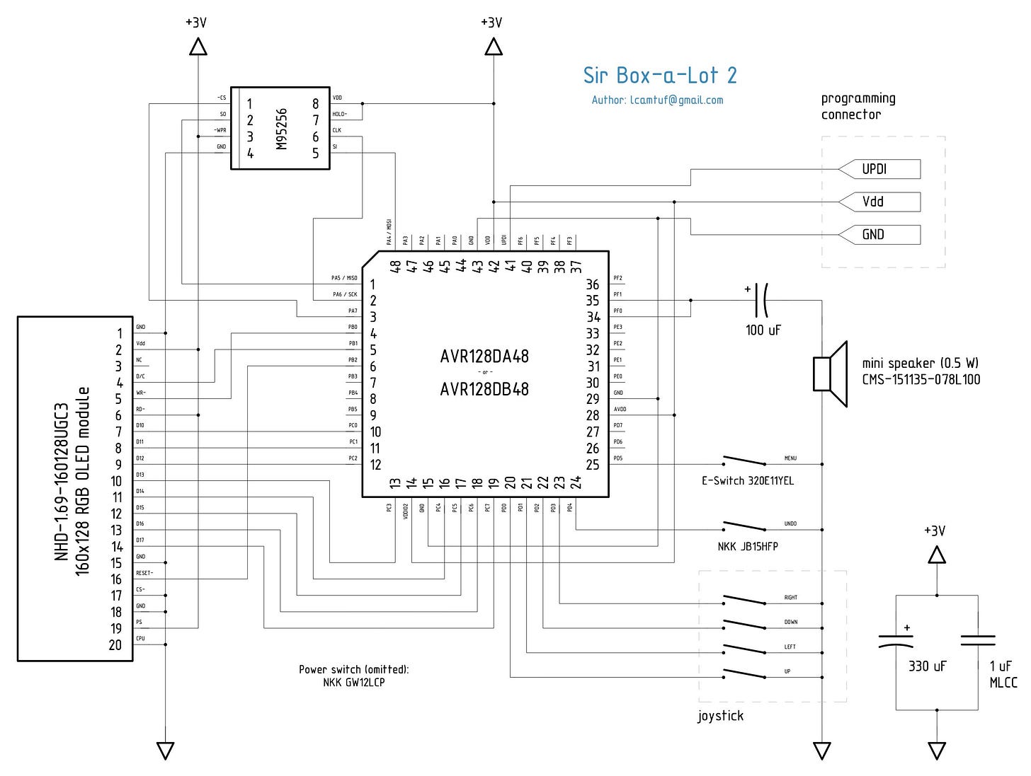
I find KiCad’s schematic tool rather unimpressive and I dislike its style of grouping IC pins by function, so I usually draw schematics in other software. Here’s what I had for Sir Box-a-Lot:
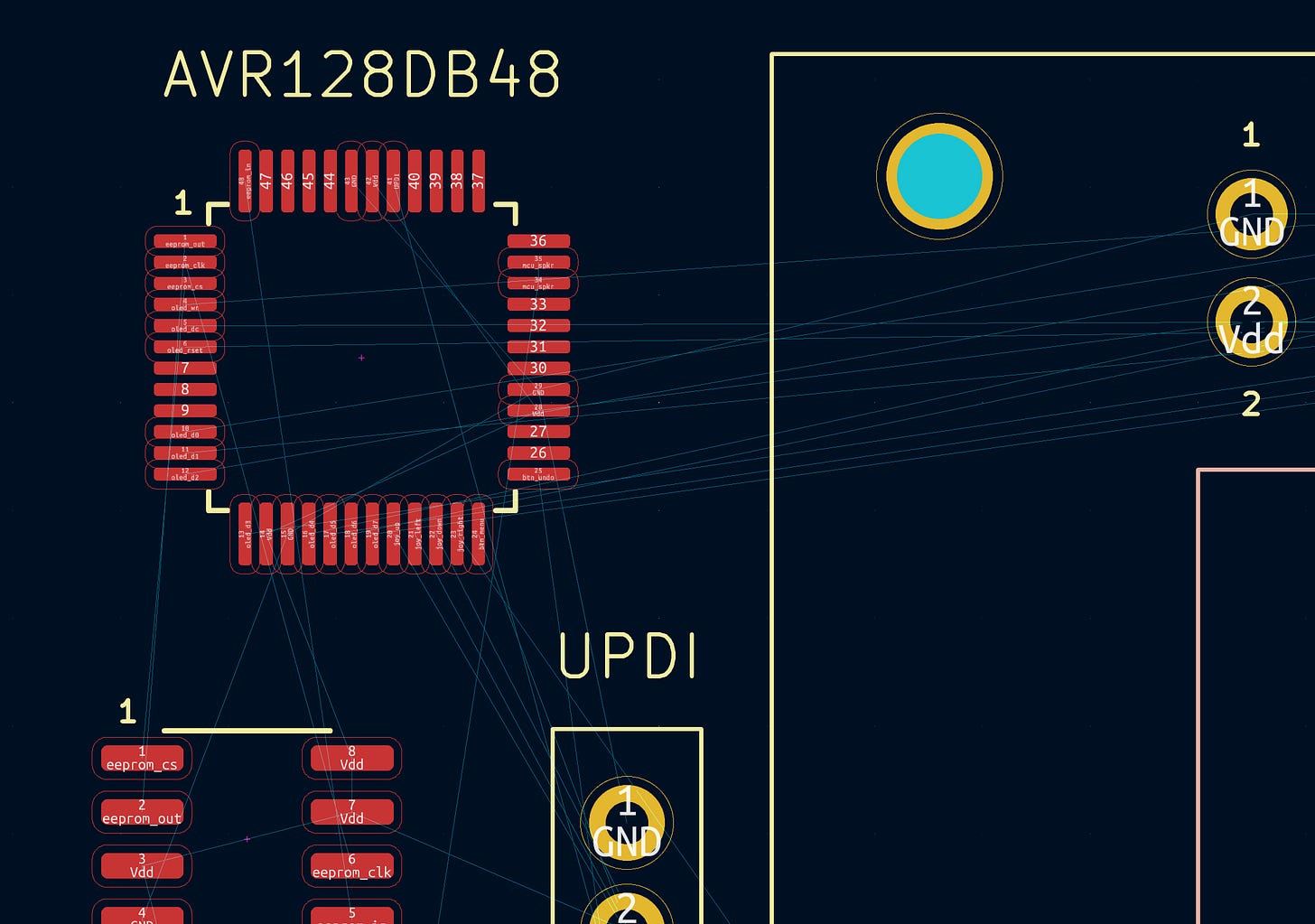
I simply used this drawing as a reference for assigning pads to nets. Pads that have a net assigned will be marked in the PCB editor with an additional outline. Once a net has two or more members, KiCad will also draw thin straight lines indicating any missing electrical connections that you now need to build by adding PCB traces. This is called a “ratsnest” view:
Step 3: refining the layout and routing traces
With all the components imported and their electrical connections defined, we can get started with actual PCB design. The first step is to define some trace widths: go to the trace width dropdown on top of the screen and select “Edit pre-defined sizes”. The list is empty by default; I suggest adding 0.15 mm, 0.25 mm, 0.5 mm, 1 mm, and 2 mm.
With this done, there are several useful keyboard shortcuts to memorize:
“X” starts drawing a new trace on the current layer,
“W” cycles through trace widths,
“Backspace” deletes the last trace segment,
“End” terminates a trace or closes a polyline,
“V” places a via and switches the trace to another layer,
“/” adjusts trace turn geometry while drawing,
“U” selects the rest of a trace after clicking on a single segment,
“D” drags the selected part without breaking any connected traces,
“M” moves the selected part and severs the traces,
“R” rotates the selected component,
“F” flips a component to the back of the board,
“-” switches between front and rear copper layers (F.Cu and B.Cu).
In addition to placing components, traces, and vias, the PCB module also allows you to add silkscreen drawings and text. Give it a whirl!
There is no one true approach to PCB layout; it’s a matter of convention and aesthetics as much as it’s a matter of science. That said, here are several rules of thumb:
Routing simplicity and debuggability should be an important consideration for component placement. For example, if the centerpiece of your circuit is a microcontroller, it might be optimal to place it smack dab in the middle of the board, and then place peripherals in a radial arrangement dictated by the location of the corresponding MCU data pins.
It usually pays to keep sensitive analog circuitry in a separate area of the PCB, away from noisy digital components, voltage regulators, radios, and so forth. If your design features on-PCB antennas, keep traces and copper planes some distance away across all layers of the board.
Power distribution traces should be reasonably wide and shouldn’t meander too much. Although even fairly thin traces can supply quite a few amps, they can exhibit non-trivial resistance, producing significant voltage drops. A standard 0.25 mm trace with a length of 15 cm will have a resistance of 0.3 Ω, costing you 300 mV at 1 A; even in a low-power design, this can contribute to excessive digital switching noise and radio interference.
Much thinner traces — commonly around 0.25 mm, but possibly all the way down to 0.15 mm — can be used for digital signal lines. It’s usually not advisable to push the limits of PCB manufacturing capabilities, so I recommend sticking to 0.25 mm unless you absolutely need to cram a lot of stuff onto a tiny board.
Ground plans or copper pours (solid copper fill areas, Ctrl+Shift+Z in KiCad) are a fashion trend in PCB design. Use them with care: there is an inherent trade-off between inductance and capacitance. When working with high-speed digital signals, minimizing board inductance with copper pours is desirable, both because it keeps RFI in check and because digital chips can overcome trace capacitance with more ease. An uninterrupted copper pour or a nearby inner-layer ground plane helps with that. On the flip side, stray capacitance hurts op-amp feedback loops and attenuates faint analog signals from microphones, photodiodes, and so on.
As a rule of thumb, for fast digital buses (above 20-50 MHz), it pays to keep data lines as short as feasible; to leave a bit more distance between the lines (for reduced cross-talk); and if there is no unbroken ground pour underneath, it pays to add an explicit return path (usually: ground) that hugs the signal trace.
By the time you cross 100+ MHz, the above rules should be followed religiously. Further, it can be important to keep the length of related data lines roughly the same to avoid signals arriving out of phase. The extent to which this matters depends on the exact rise times and the design of the protocol, not on the clock speed alone; in practical terms, it’s an important consideration for protocols such as USB 3.0, HDMI, or MIPI-CSI.
Sharp turns and unusual trace angles are frowned upon by PCB designers. Most of the time, this doesn’t matter as far as electrical properties go, unless you’re in working on microwave circuitry — but evenly-spaced 90° traces with chamfered 45° turns are what people have come to expect. Go with the flow, it makes you look like a pro. In KiCad, pressing Shift+Space constrains all drawing to 45° stops.
On surface-mount PCBs, vias are indispensable for efficient routing — and contrary to some internet lore, it’s almost always OK to use them liberally. The resistance of a typical via hovers around 1 mΩ, but they don’t dissipate heat well — so in high-current applications, multiple vias can be “stitched together” with a trace.
Modern-day PCB manufacturing techniques also impose handful of practical constraints:
Minimum trace size and minimum trace spacing is usually around 0.15 mm.
Minimum hole diameter is typically 0.3 mm for low-cost PCBs, and around 0.15 mm if you’re willing to pay more. Minimum overall via size is commonly around 0.5 mm for standard boards (this includes the annular copper-plated area around it).
A margin of around 0.25 mm must be maintained around holes; minimum hole spacing is usually around 0.5 mm. You should keep more generous allowances around mechanical holes: metal fasteners can short or damage nearby traces.
Once you have the board designed, you should mark its perimeter. Most simply, this is done by drawing a rectangle on the Edge.Cuts layer; more fanciful shapes are possible too. On the account of manufacturing constraints, a setback of at least around 0.5 mm should be maintained between the edge and any board features.
Step 4: rule checking and visual inspection
With the PCB design done, it’s time to inspect the result. First, enter physical design constraints by opening the “File” menu, selecting “Board Setup”, and going to “Design rules → Constraints”. You can enter the dimensional rules discussed above, or pick other values dictated by the board manufacturer or appropriate for your design.
Next, go to the “Inspect” menu and select “Design Rules Checker”, then click “Run DRC”. This analysis will alert you to a variety of potential manufacturing issues, including layout constraint violations, unintended connections between different nets, or — most likely! — some overlooked pad that isn’t electrically connected to its designated net:
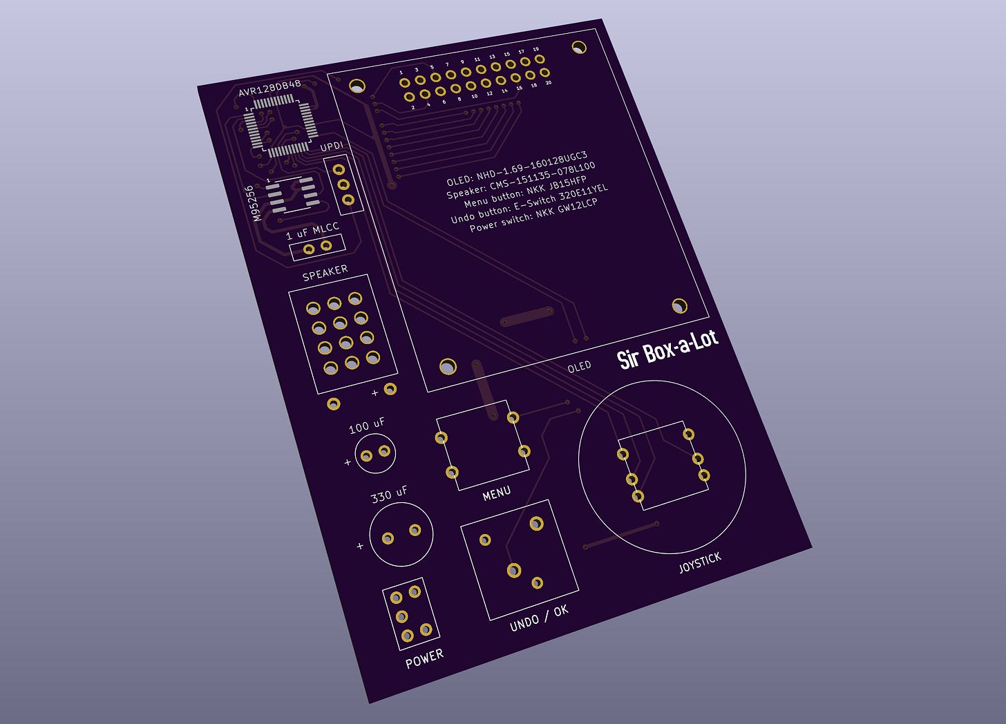
The next part is a visual inspection in the 3D viewer. Press Alt+3 and look closely at the front and the back of the board, making sure that all the soldering pads are exposed, all the holes are where they are supposed to be, all the graphics are on the silkscreen layer, and that nothing else looks off. Confirm that there is no important silkscreen over holes, pads, or vias.
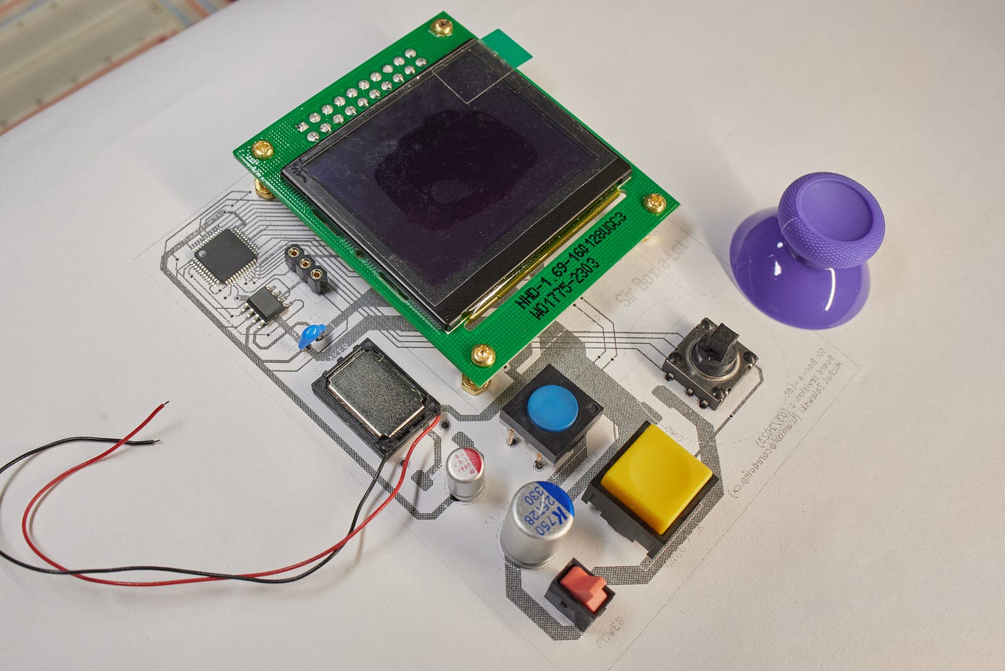
You want to be certain the board is perfect before you send it off to the manufacturer, so I also recommend printing out design on paper (at 1:1 scale) and then testing for component fit. It’s possible to pick the wrong footprint from the standard KiCad library or fat-finger a dimension for hand-drawn parts — and this simple if goofy experiment can save you 1-2 extra weeks of waiting:
Step 5: sending your PCB to a fabricator
To generate production files, go to the “File” menu, select “Fabrication Outputs”, and then “Gerbers”. Specify a new output directory and click “Plot”. Next, without closing the dialog, select “Generate drill files” and then press “Generate”. At that point, you should have a directory with about a dozen text files. Put everything in a simple zip file and voila!
What to do with the zip file is another matter. Perhaps the most hobbyist-friendly and dependable PCB manufacturer is JLCPCB in Shenzhen, China; their usual turnaround is 1-2 days, plus about 3-4 days for affordable shipping via DHL; if you’re lucky, the board should arrive within a week. The total price tag for a bunch of Sir Box-a-Lot boards ordered with JLCPCB would be about $30.
There is a good number of PCB factories in the United States, but they aren’t particularly interested in catering to hobbyists, and are likely to quote you several hundred bucks for a short run. The best US-based option is OSH Park, an intermediary that pools orders from multiple individuals, combines them into one large panel, ships the order to a manufacturer, and then sends you back the result. That said, the whole process is necessarily slower and more expensive than working directly with a fabricator. In other words, depending on the strength of your geopolitical convictions, you have an interesting choice to make. With OSH Park, you should probably budget closer to $50 and be ready to wait two weeks.
The ordering process itself is simple: you upload the archive, make a couple of consequential selections (such as choosing your favorite solder mask color), visually confirm the result, pay with Paypal or a credit card… and then sit back and relax.
👉 To download CAD files and source code for the project, click here. For a mini-review of hobby PCB vendors, go here. To explore SMD component footprints, see here. To check out earlier electronics-related articles on this blog, visit this page.
I write well-researched, original articles about geek culture, electronic circuit design, and more. If you like the content, please subscribe. It’s increasingly difficult to stay in touch with readers via social media; my typical post on X is shown to less than 5% of my followers and gets a ~0.2% clickthrough rate.




What software do you prefer for schematic design?
I have been really impressed with JLCPCB's free EasyEDA editor and its integration with the voluminous number of competitively priced parts, footprints, and 3D models associated with their very reasonably priced pick and place service. It feels like a well-oiled hangout spot for hobbyists where it's easy to publish designs open source and collaborate, discover what parts people are buying by sorting by quantities at https://jlcpcb.com/parts/all-electronic-components, and now it has a seemingly reasonably priced 3D printing service too (includes MJF and SLS)! It's very low friction for my small-sized projects. I can go into more detail if you'd like.
The costs feel subsidized compared to American prices for these things, but I don't know how I would find out the truth :) I'd like to visit in the fall, I'll see if they'll let me!